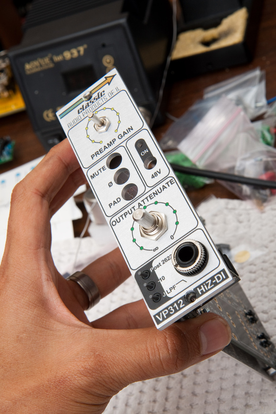
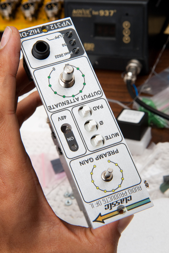
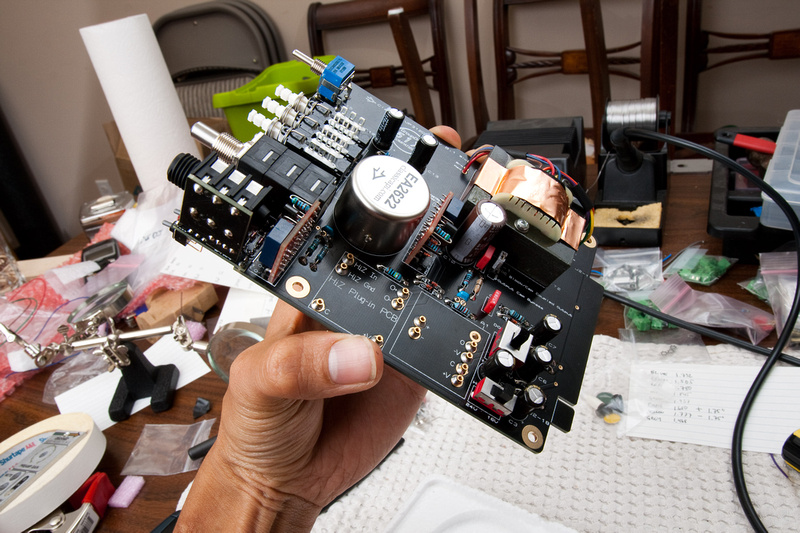
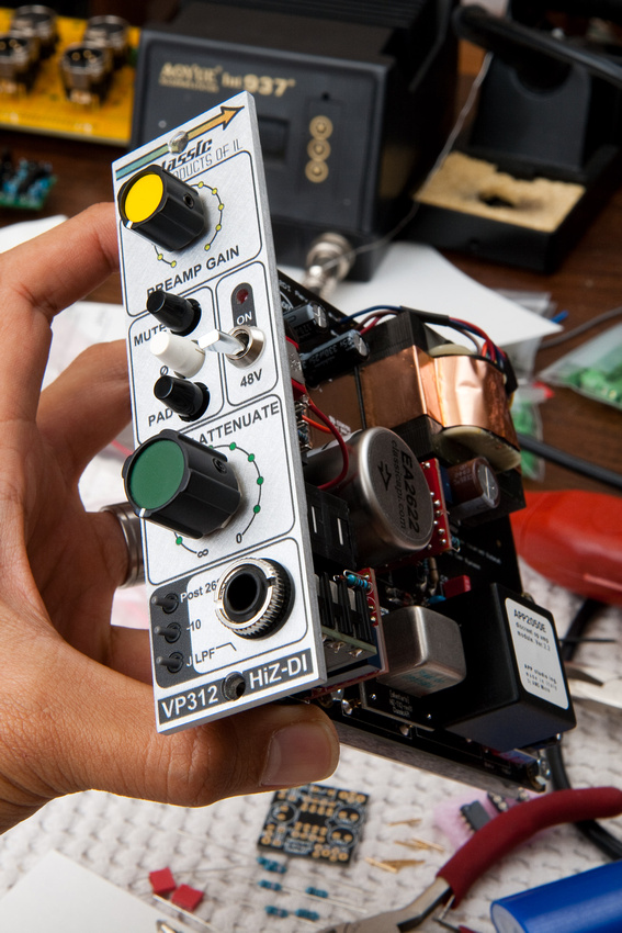
So, in short, there are a mind-boggling array of possible configurations for this preamp kit that can all be changed quickly and without soldering. For this build, I will explore a few of them.
opamps: GAR2520, APP2520E (+/- 24V)
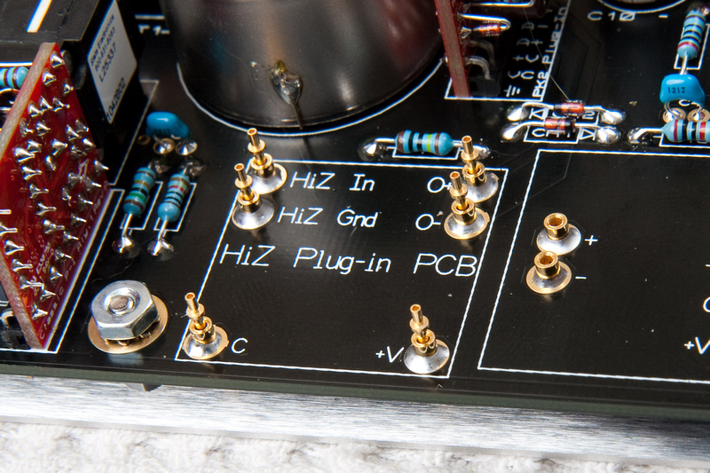
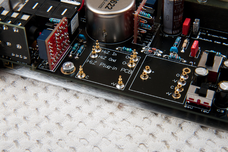
DI modules: FET DI, Picatron passive transformer DI, and the IC chip DI
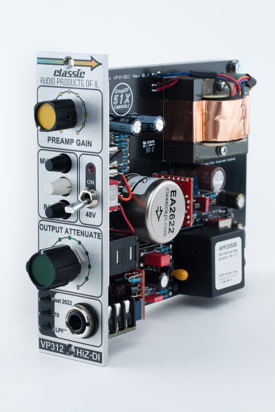
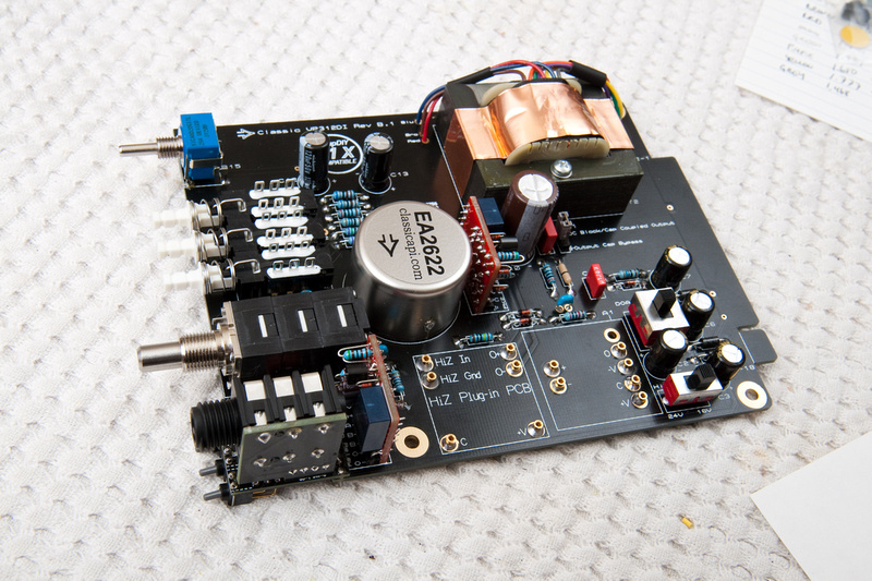
The current revision of the VP312DI preamp has a new option on the PCB for stepped resistors on the gain knob, so you can now choose between the constant variable Bourns pot (as depicted in this older revision build) and the Grayhill switch with stepped resistors when purchasing this kit.
There is no in-depth step-by-step assembly guide for this build, but a lot of critical build information is consolidated in the official support thread on the http://www.groupdiy.com forum. All of the critical build documents (schematics, bill of materials, and assembly guide) are also sent via email upon purchase. In this post, I will attempt to detail every step of the VP312DI kit build.
When I first approached Jeff Steiger about building this preamp kit, he suggested I try the VP26 kit first because it has fewer components and is more newbie friendly. These were among the very first DIY electronics kits I had attempted, and I was quite glad I followed Jeff's advise as the VP26's are brilliant sounding preamps with a different sonic footprint than this VP312DI. Easily the most difficult part of assembling these two fine preamps was tackling the GAR2520 opamps as the parts are very closely packed. It is my hope that these step-by-step build threads will allow those on the fence about DIY to take the plunge.
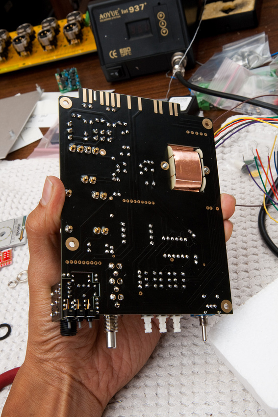
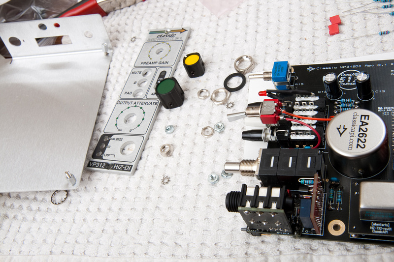
With that, here are the contents of the VP312DI package that I received.
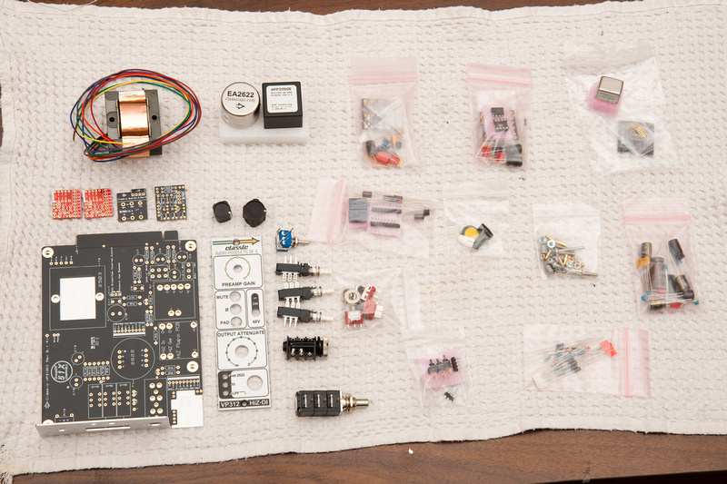
After identifying generally how everything was organized in the baggies, I figured I should identify and sort parts first. I grabbed my cheap multimeter and pulled up a capacitor ID chart as well as a resistor color code chart on my web browser and got busy sorting. The bill of materials documents are organized by PCB, so I pulled up the PDF for the main board first. The baggies that contained the DI kits seemed all self contained, so I set those aside for now.
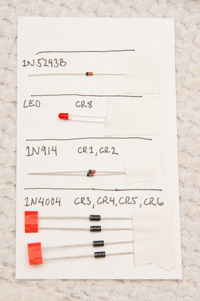
I started with the diodes. (note:I'm going to go ahead and apologize now for the size of some of the upcoming images. I figure clarity trumps load time. This forum does not seem to auto scale, so I will try to be cognizant of typical display resolutions.) To organize, I used some 3x5 cards a pen, and some console tape. I'm sure there are probably more efficient methods to be had, but this seemed like the thing to do at the time.
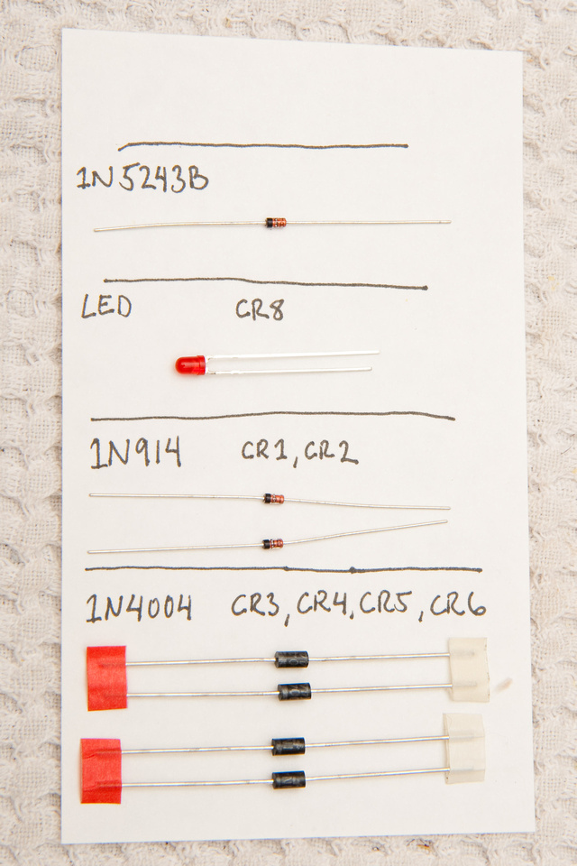
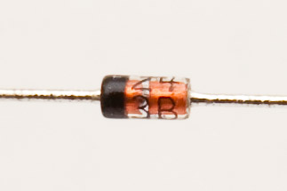
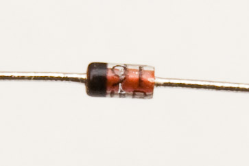
ok. . . I just realized I did not label CR7 (1N5243B) [top one in the above picture] on my card prior to shooting all my photos. The markings on these things are absolutely minuscule and the clear body with contrasting internal colors does not help a bit. What I wouldn't give for a macro lens right now. . Here's what they look like:
labeled:
24
3B
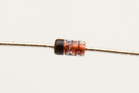
CR1 and CR2 (1N914) look like this:
labeled:
91
4B
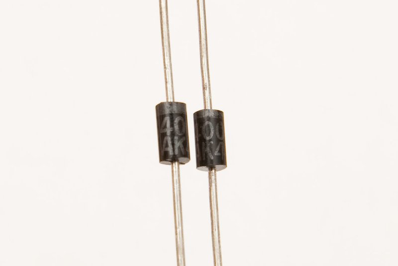
CR3, CR4, CR5, and CR6 (1N4004) are much easier to identify
A few strips of console tape secure these diodes to the card for easy access later.
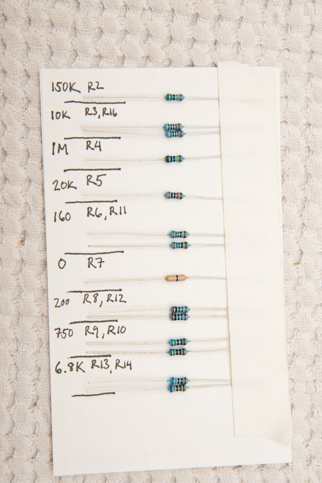
Next, I sorted my resistors checking both on multimeter and color code chart. Hopefully I got these right. Again, a piece of tape secures these to the card.
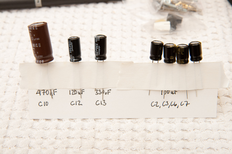
Next, I identified my electrolytic capacitors which was easy as they are all clearly marked in legible print.
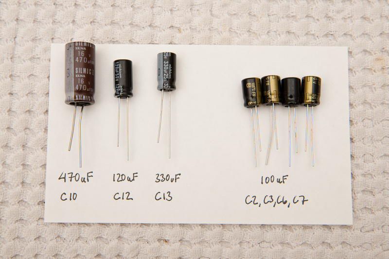
And add a bit of tape to secure them.
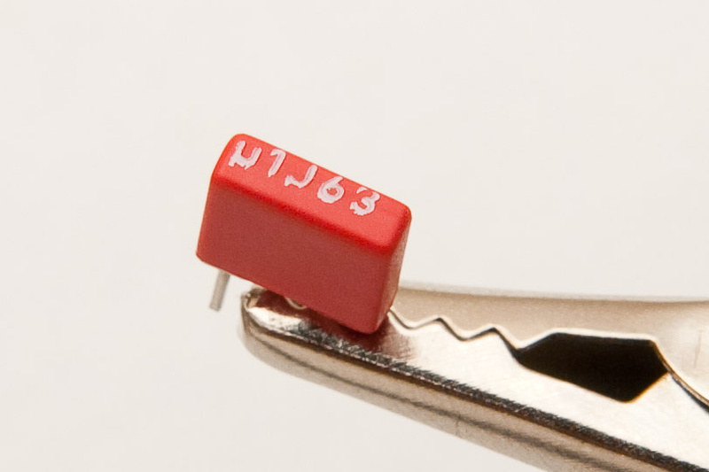
And, same for the film and ceramic caps. The markings on the blue caps are somewhat difficult to read, but not as hard as the diodes.
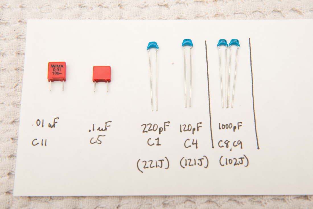
C5 (.1uF) is marked like this:
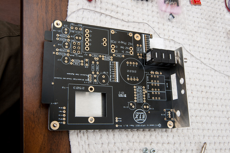
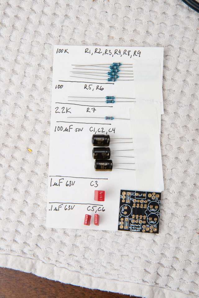
And, I have identified and sorted the parts for the main PCB. A few components from the baggies I opened are unaccounted for. I think those will probably come into play on one or more of the smaller PCB's in the build. But, for now:
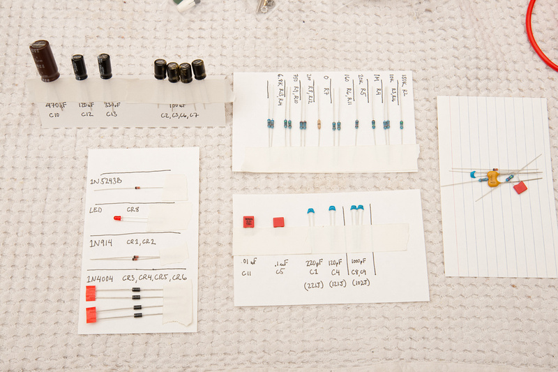
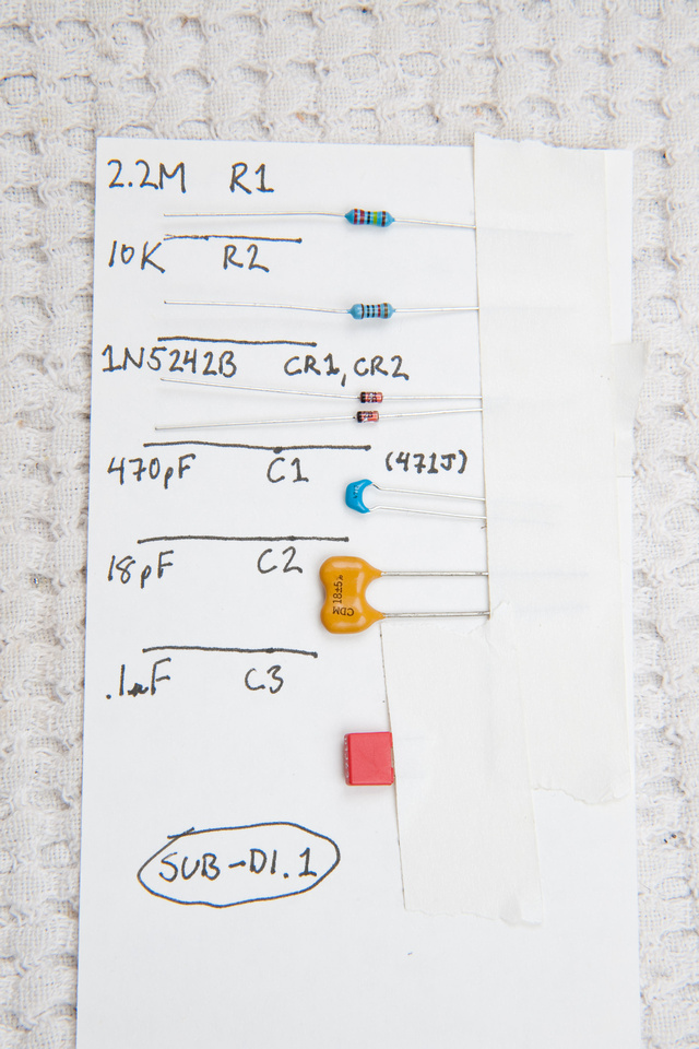
one more set of parts to sort before I can start sticking stuff together. I figured out what those "extra" parts were. I know it's one thing to have "extra parts" when you put your car back together, but I figured electronics is a different animal. These are the parts for the "sub-DI" board:
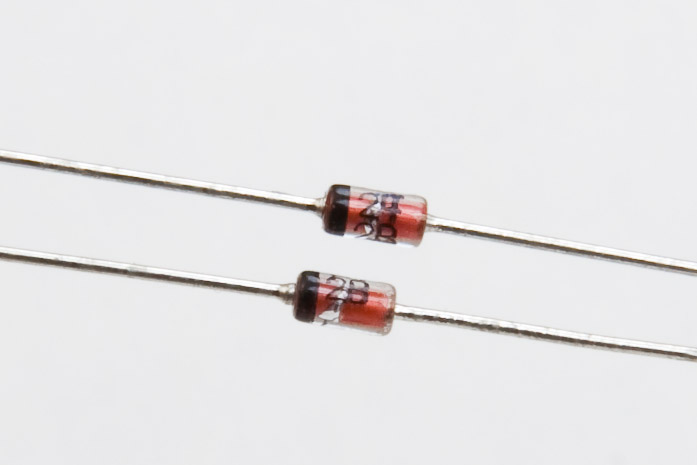
CR1 and CR2 (1N5242B) look like this:
label:
24
2B
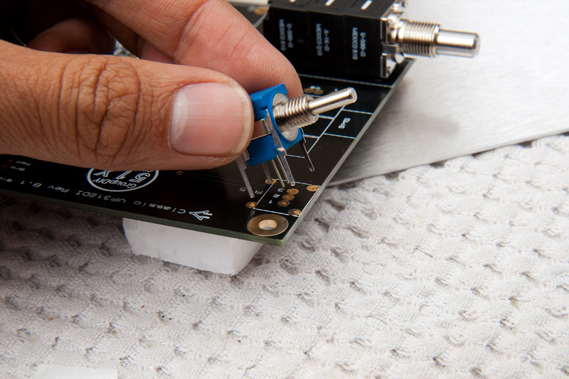
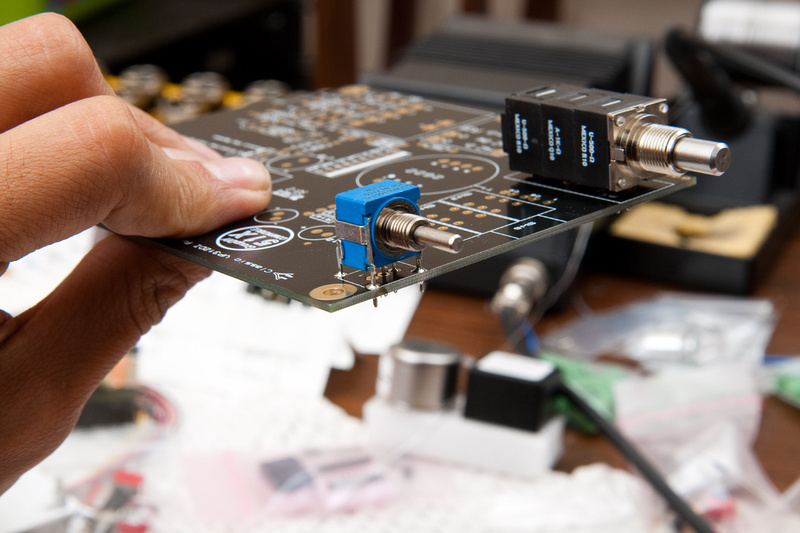
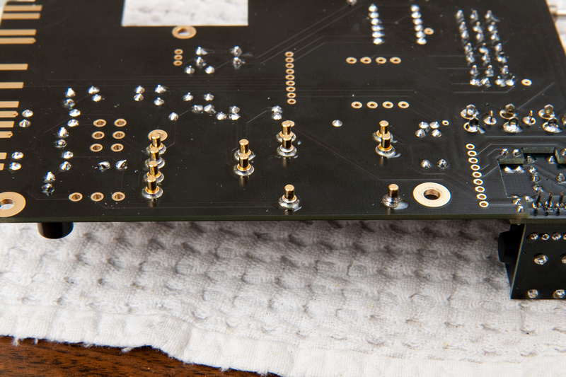
Main board components are accounted for. Following Jeff's pointers on the official support thread, I use 2 of the smaller PCB's as spacers for the output attenuator pot.
A bit of console tape helped me keep everything together so I could solder a couple of lugs.
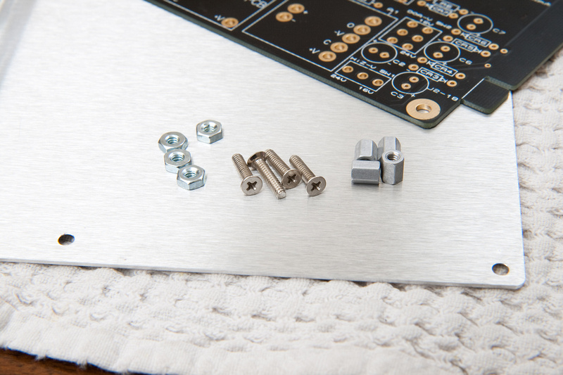
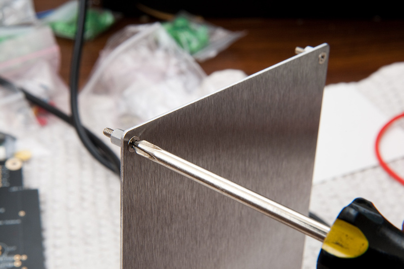
I then found these standoffs, screws, and nuts to mount the main PCB onto the aluminum L bracket to test the fit before I solder more lugs.
I tighten down the rear standoffs to final torque. They will not be coming back off if all goes according to plan.
The front ones go on loosely so the screws do not protrude above the standoff. this is so you can slide the knobs through the front panel holes without interference.
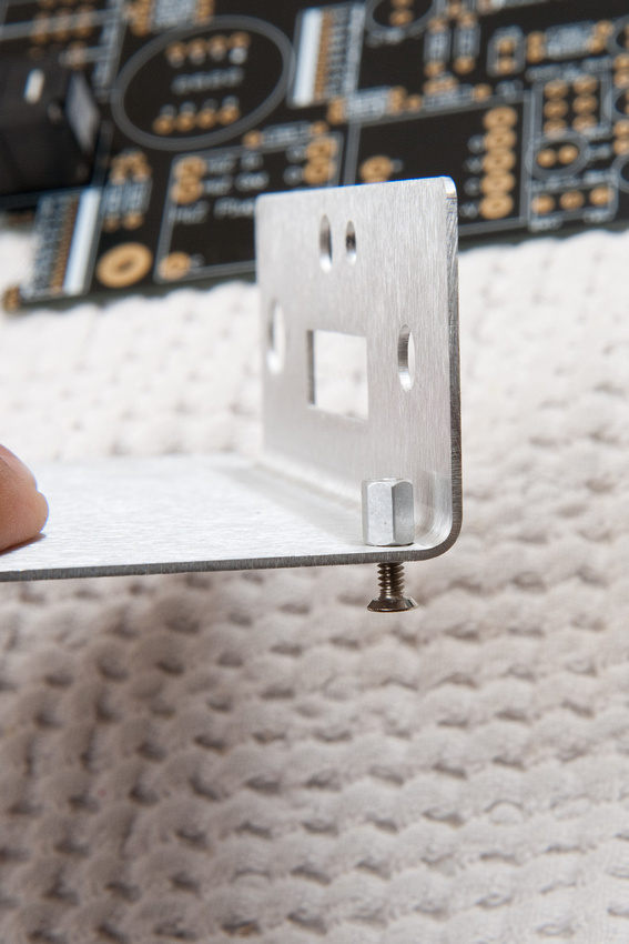
the PCB should slide into the bracket and align with the standoffs like this:
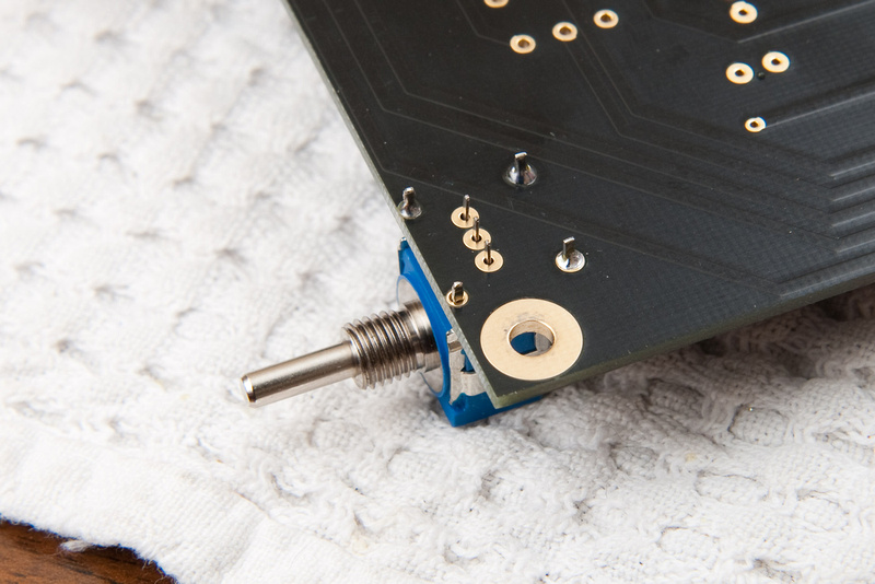
The height of the pot in relation to the L bracket and the PCB looks good.
I then remove the PCB from the L bracket and solder all of the lugs on the output attenuator pot. After this, I place the preamp gain pot but don't solder anything yet.
I re-assemble the PCB and L bracket again without soldering the preamp gain pot yet.
I assemble this time with the front panel to precisely align the preamp gain pot to the chassis prior to soldering.
Notice the spacing on the reveal between the L bracket and the front panel. In all of these parts alignment procedures, I'm trying to make that small reveal at the top of the L bracket parallel with the front panel.
I am able to reach 3 lugs without much difficulty, so I solder those with the PCB/chassis assembled to lock in the position of the gain pot.
and, soldered in.
Then I take it apart again and solder the remaining lugs.
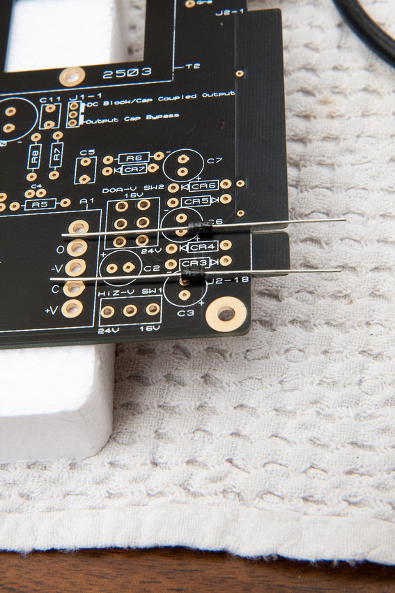
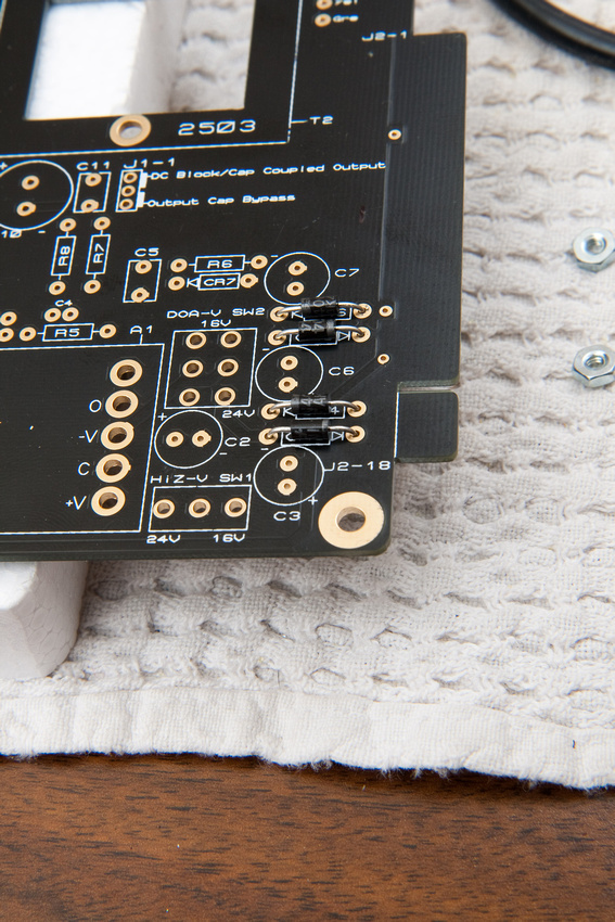
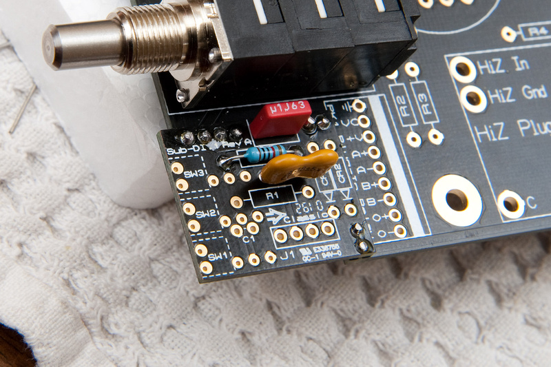
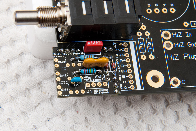
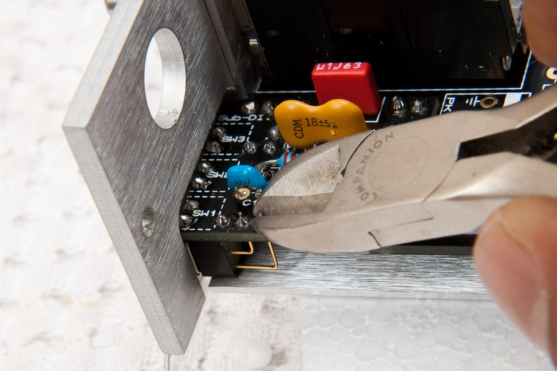
Next, I install CR3, CR4, CR5, and CR6 because I need the cut-off legs from these diodes to mount the small DI sub-board to the main PCB. Polarity matters when mounting the diodes. Makes sure the end of the diode with the solid line corresponds with the little arrow mark on the PCB when mounting these.
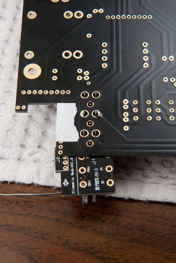
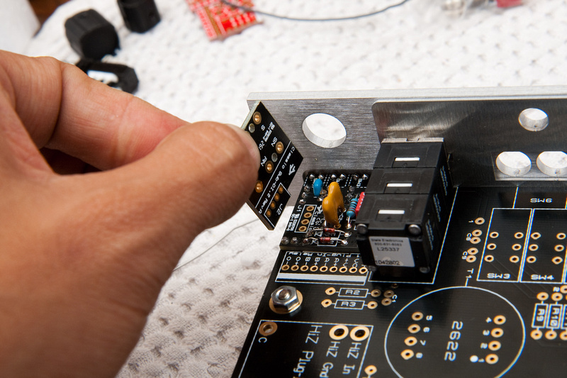
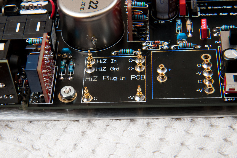
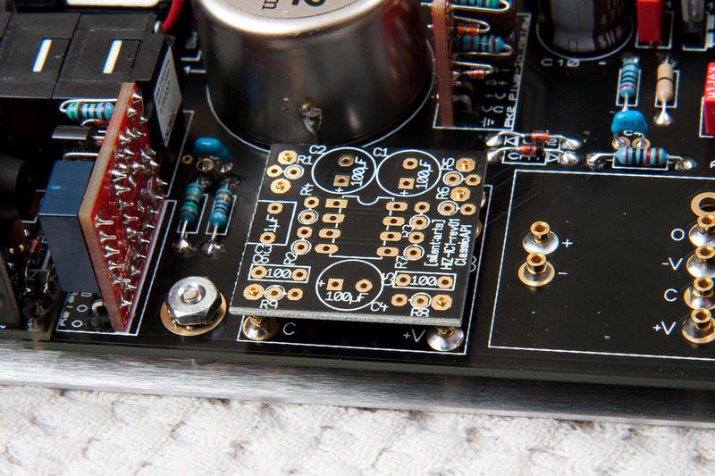
The small DI sub-board goes here:
Per Jeff's notes in the support thread, I secure 3 corners first. Except I did not populate the board prior to assembly. I figured it would be easier to clamp without any components mounted, and a quick study of the board seemed to indicate I would not have any problems installing any necessary components after it is attached to the main PCB.
I used 2 clamps to ensure solid contact between the 2 boards prior to soldering.
. . . and corners are tacked in.
The rest of the appropriate holes are filled . . .
. . . and the 2 boards all soldered together.
After the boards are solidly attached, I set about populating the DI sub-board.
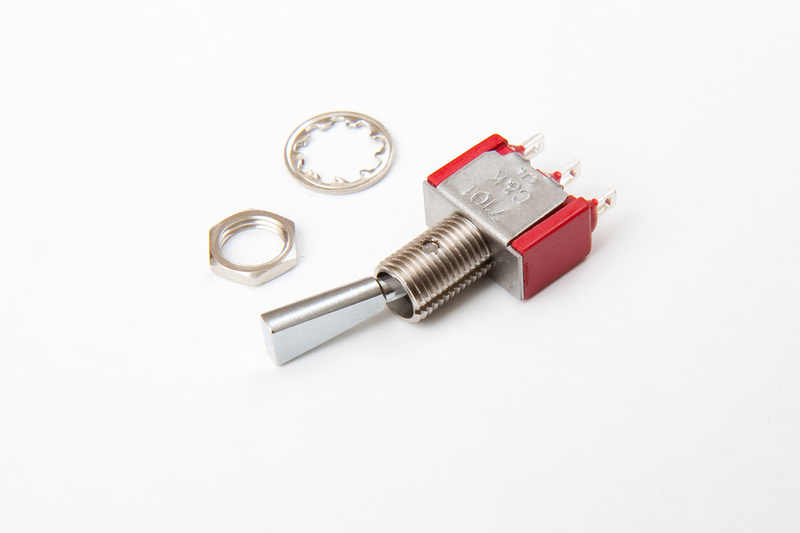
The 3 small toggle switches that control DI functions look like this:
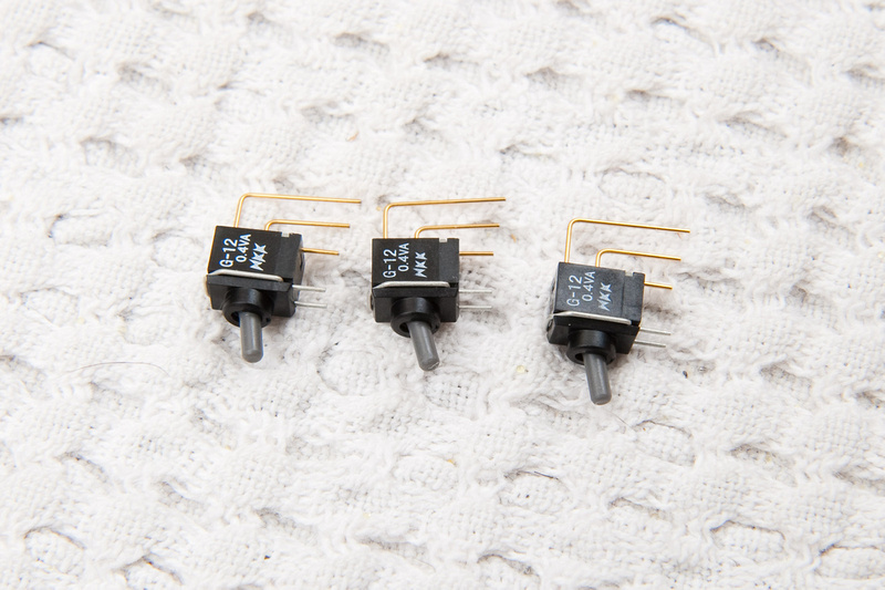
They are a bit tricky to position for mounting. I ended up securing them like this:
and then, I added a piece of tape to put some downward pressure on the main PCB so the switches pressed firmly against the PCB.
I then soldered only one of the main mount lugs on each of the switches so that fine adjustments could still be made to the final position.
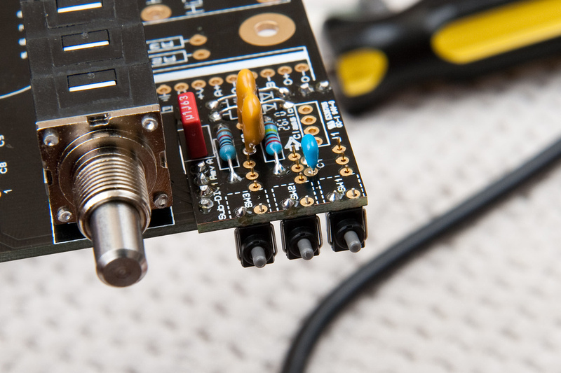
Then, it was back to re-assembly to make sure everything was lining up still.
. . . and I decided I could reach all of the switch solder lugs with the chassis attached. So that's how I soldered them in.
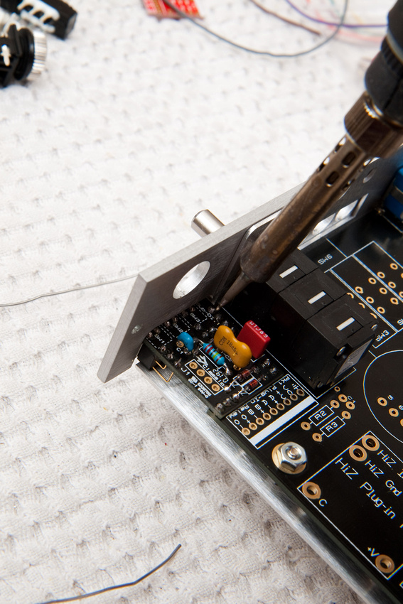
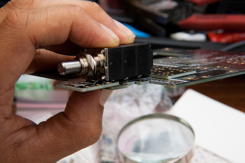
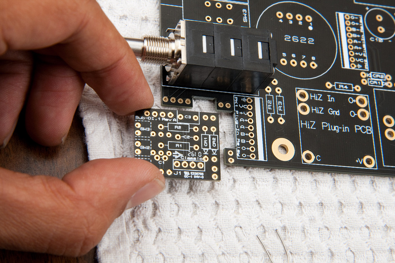
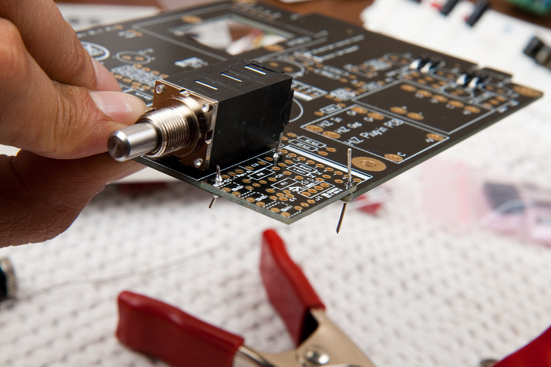
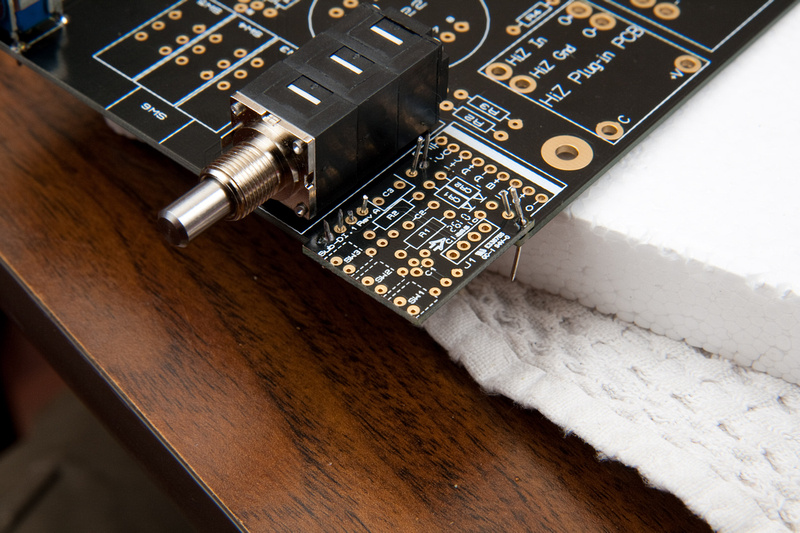
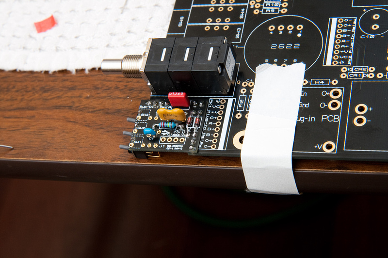
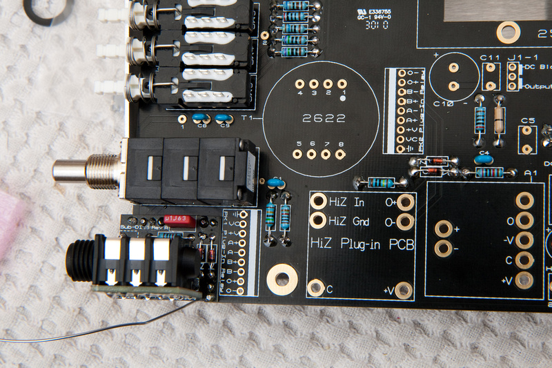
Jeff's notes said the pins for SW1 need to be trimmed to fit the small PCB that supports the 1/4" jack.
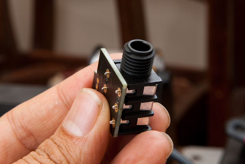
That small PCB goes here:
And the jack mounts like this. . .
Jeff's notes warned about the possibility of the PCB being longer than the jack housing, and mine was by a hair, so I used some 220 sandpaper on the table to grind down a little bit of the PCB's front edge.
. . . good to go.
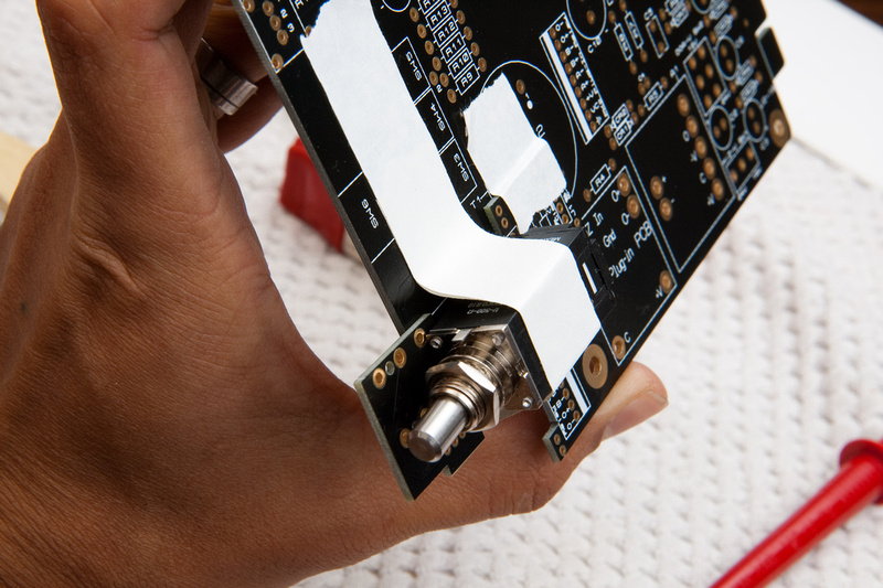
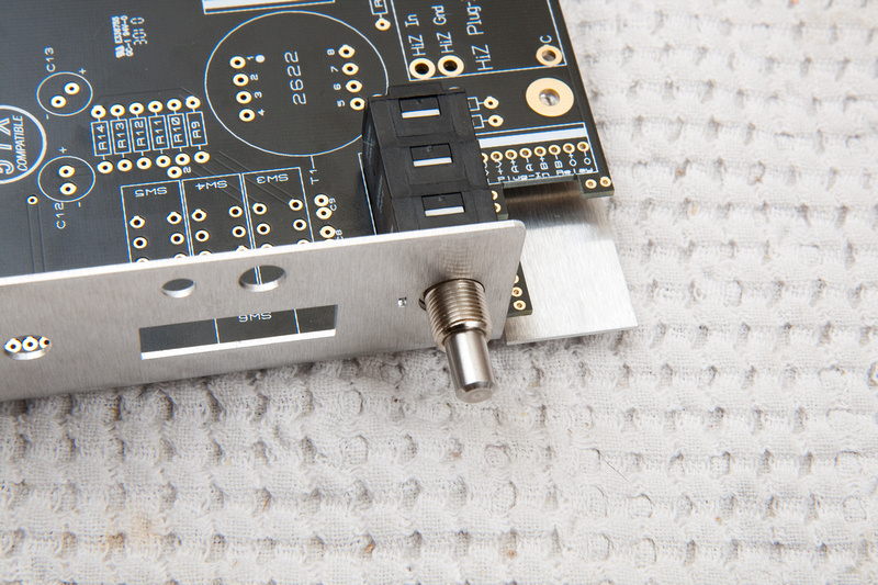
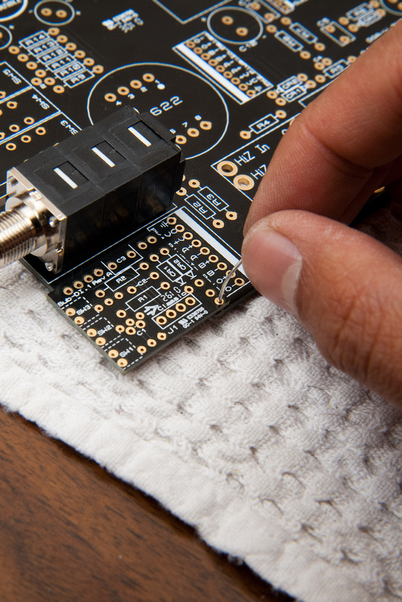
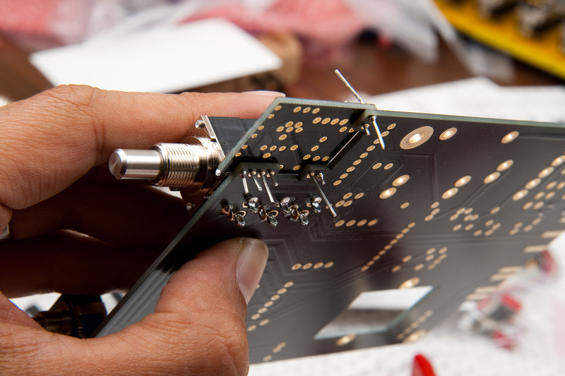
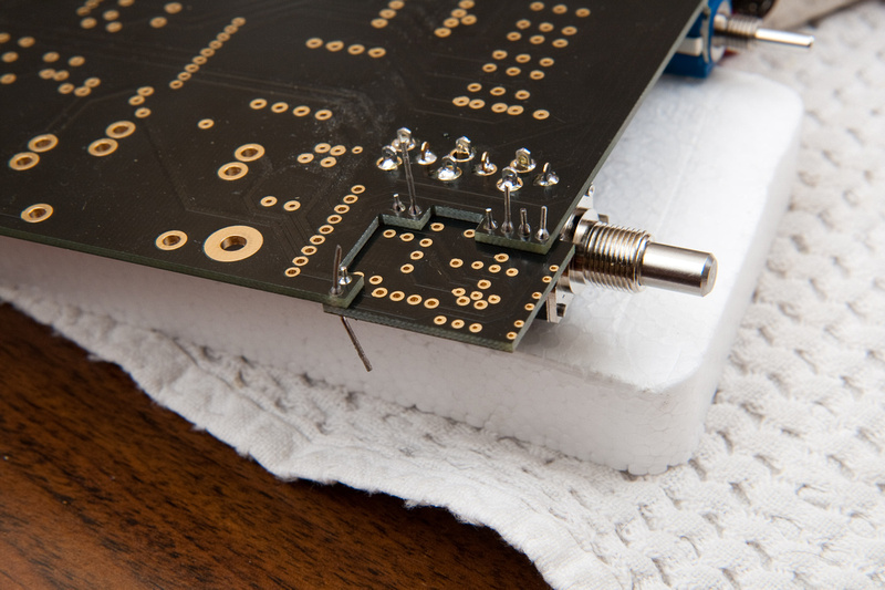
I think I did the next set differently than described in the support thread, but it seemed to have worked out. First, I placed the connector without soldering.
Then, I inserted the jack/PCB (also not yet soldered together) into the front panel hole at an angle. . . and then rotated the assembly into the connecting pins.
I then secured the nut for the DI jack to lock everything in place.
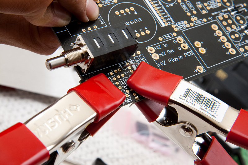
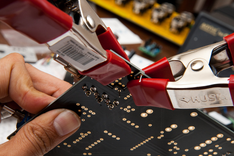
The way I saw it, I could reach all of the significant solder lugs from the outside with the PCB attached to the chassis and the jacks/pots attached to the faceplate. I thought that would give me the best shot at perfect alignment of parts, so I soldered everything with the front panel attached.
Progress. . . all of the key front panel elements are now precisely aligned. From building the VP26, I know the 3 push button switches have a lot of margin, so chances are, they will not be problematic if the rest of the pots and switches are aligned with the PCB, L bracket, and front panel reasonably well.
Next, I place the mute, phantom power, and phase reverse buttons. These gave me grief on the VP26 because I didn't set them right the 1st time. In hindsight, it would have been fine to just leave them as originally installed instead of re-heating and mechanically buggering the switches (pushing so hard the pins got pushed upwards in the housing. . . and then I had to re-heat and press them back down). This time, I made sure the little plastic tabs were touching or darn close to touching the PCB before soldering anything.
And then, I only soldered in 1 pin on each connector at first. . .
. . . so I could re-assemble the PCB to the L bracket and faceplate to verify what I already knew would be the case. . . the buttons are sitting fine. Well, the preamp looks all upside down, but besides that, everything is fine.
Next, I dis-assembled the preamp again and soldered up the push-button switch lugs. Jeff recommended a soldering sequence in the VP26 manual, but I just made sure I jumped around like I was A.D.D. when soldering these in hopes of not overheating any single component.
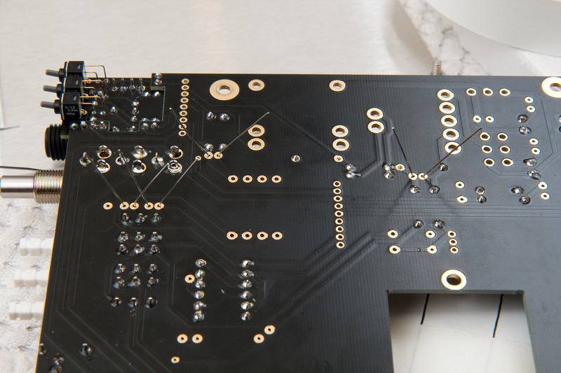
At this point, I believe all of the mechanical components that can cause you grief in physical assembly if mis-aligned have been set. So, I thought it would be a good time to start populating the main PCB. I went with resistors first. Since I had already pre-sorted my components, it was now a simple matter of locating the marked slot on the PCB and plucking he right part from my little 3x5 cards. It's sometimes confusing when you don't have some sort of step-by-step instructions to figure out what to install first. Everything on the PCB looks pretty accessible, but the reasoning behind my particular sequence was to start low on the PCB, and install those low components first. . . then, install higher and higher ones because the high components could potentially hinder me from reaching a lower component.
Then, my diodes. . . (Note: polarity is important for diodes. . . each one will have a stripe on one side. Make sure to align the stripe side of the diode with the little arrow marker on the PCB.)
Then, my ceramic capacitors.
For the ceramics, I ended up bending the leads outwards to secure the component and then soldered from the back side as opposed to from the front side for the resistors and diodes.
chop choppy.
I was trying to figure out how to keep the film capacitors from falling out of the PCB when I turned it over to solder, so this is what I ended up doing.
And, the film capacitors are in.
Then, the radial caps. . . each position on the PCB is marked + and - . I made sure the vertical strip on the caps with the "-" sign in it aligned with the - terminal on the PCB for each of the Radial caps. I hear this is important.
And again, like with the ceramic caps, I bend the leads to hold the radial caps in place to solder from the bottom.
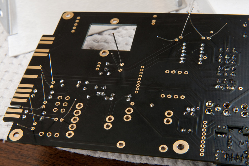
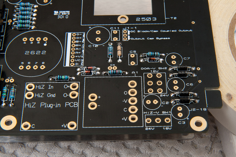
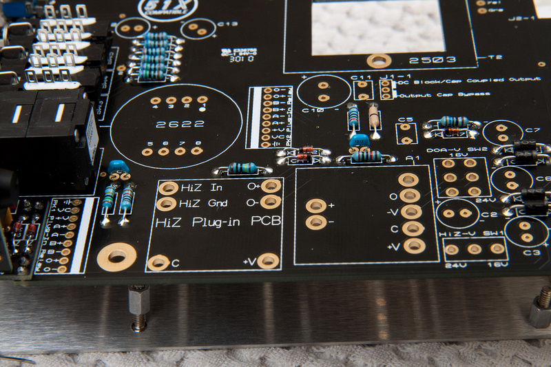
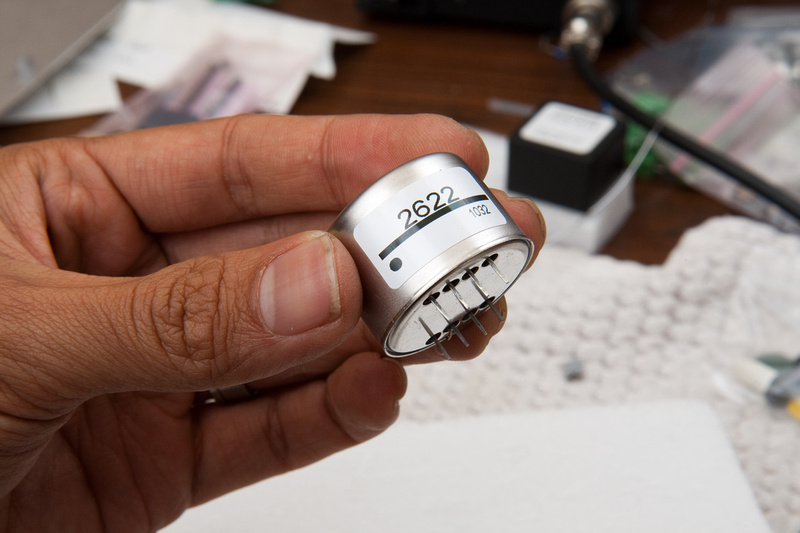
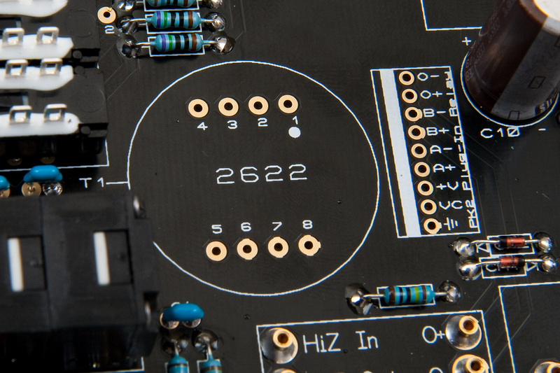
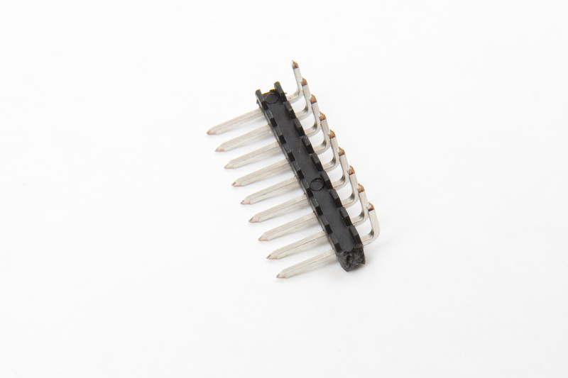
Next, I dumped out a pile of pretty little socket connectors for the op amp and DI plug-in modules.
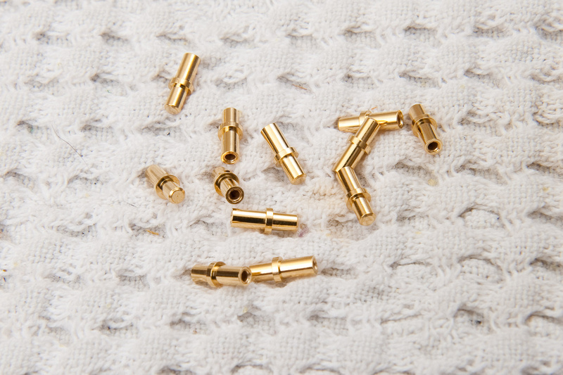
Jeff's notes indicate that it's important to install all of these from the bottom side of the PCB. Notice one of the holes does not require a socket. This one does not have any markings next to it on the front side of the PCB because, well, I guess it doesn't have a function?
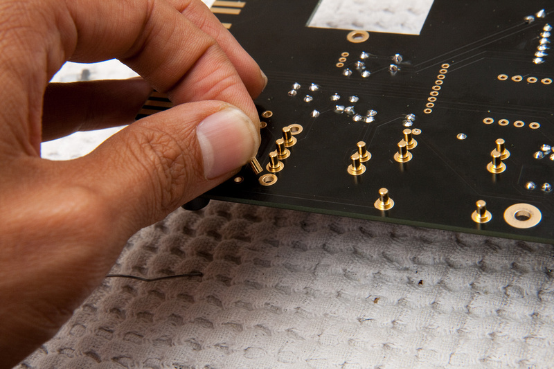
When soldering these little buggers, I turned up the heat on my soldering iron. . . (Note: I'm not sure this is a prudent thing to do, but those lugs looked hug and the pins have a lot of thermal mass). I upped the juice to 380 degrees Celsius on my temp-regulated iron (that has stopped me from burning up a lot of bass guitar pots). I head at the seam between the socket and the PCB lug and continue to apply heat until I see solder run down the PCB lug hole and feed quite a bit more solder through than I would a normal component. I want to create a strong solder fillet on the front side and the back side of the PCB in one go so the sockets have no chance of slipping out as they will be mechanically stressed when inserting and removing modules.
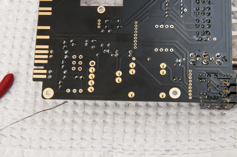
And, this is how the front side looks keeping in mind this was 1 pass, meaning I didn't touch up any of the lugs from the front side because if I melt the solder, the socket would fall right out if soldering from the front side. This ensures that there is solder within the full length of the PCB lug as well as on top and bottom. Some are better than others because it's a blind process, but I made sure there was "something" on all of them.
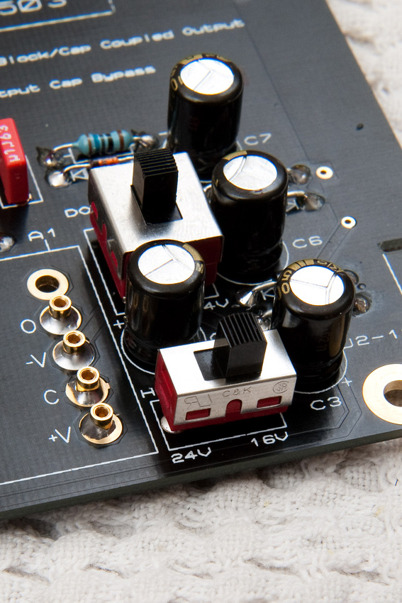
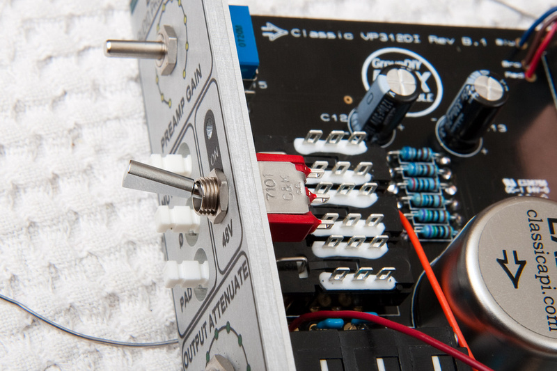
Next, I installed the switches that toggle between 16V and 24V for the op amp and the DI module. I'm so glad this design fully utilizes the 51x feature set!
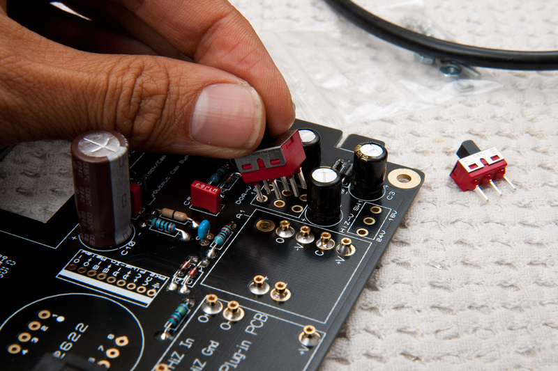
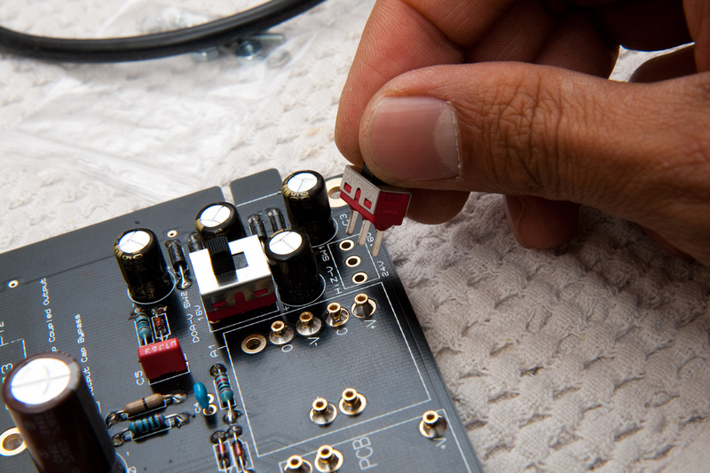
And again, tape to the rescue to hold these on while I solder from the back side of the PCB.
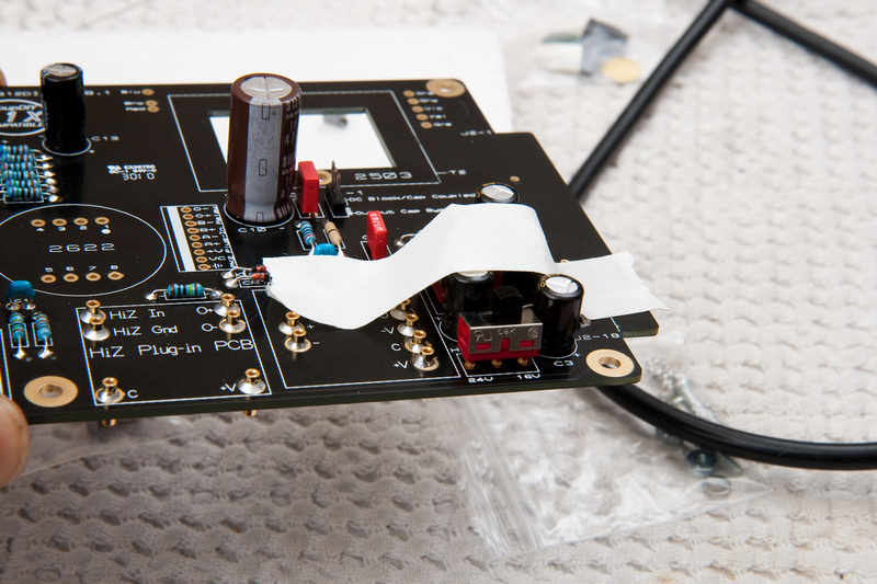
Voila!
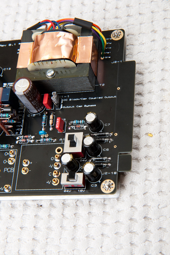
Up next for no apparent good reason except it needs to get done at some point is the input transformer. Note the black dot on the sticker indicating pin 1.
Note the dot on the PCB indicating pin 1.
It's critical to install the transformer with the proper orientation.
Jeff likes to use double-stick tape under the input transformer. Poor folks like myself don't have access to such fancy pants items, so I ended up getting some electrical tape and making a little donut with it sticky-side-out . . . elementary school style.
The white tape indicates pin 1 since I obscured the PCB markings and I don't want to muck this up because i have no idea how I'd get the transformer out after I stick it in.
And, humans win!
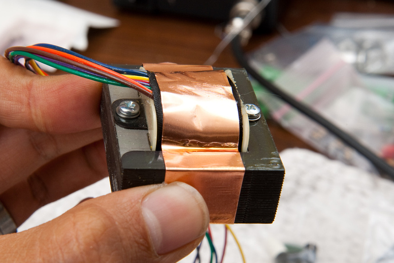
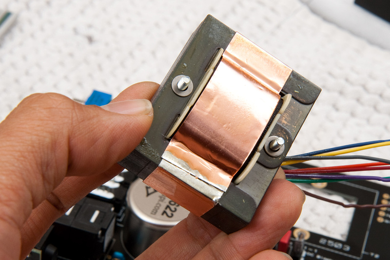
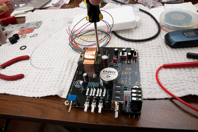
While I'm doing transformers, I figured I'd move on to the output transformer next. First, I went to dig up these parts from the appropriate baggie.
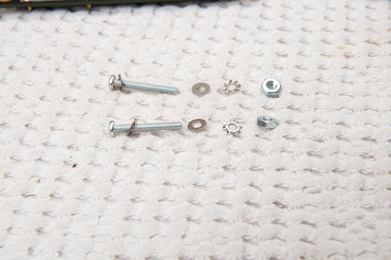
Screws go into the top side of the transformer with a flat washer between.
I then flipped the transformer over and placed flat washers on the under side as well. These flat washers will contact the PCB.
I found the easiest way to get the thing placed was to turn the PCB on its side and mount the transformer this way. . . make sure the wire leads are on the top side of the PCB. . . well, I guess you could install it with the wires pointed down, but it wouldn't be as clean. (side note: it's extremely difficult holding a large DSLR camera with sizable lens in left hand while trying to place transformer with right hand.)
OK. . . now, all I have to do is grow a 3rd arm and throw a lock washers and nuts on those screws from the back side. (and don't forget to take some pictures
 )
)
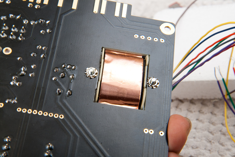
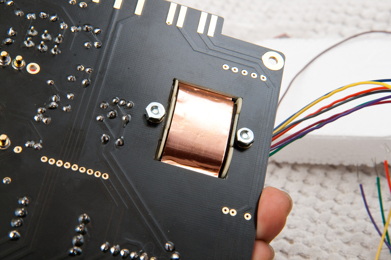
The nuts go finger tight so I can turn the PCB over and line up the transformer with the lines so it looks pretty.
when it's all lined up, I torque down the screws. . . not too tight . . . not too light.
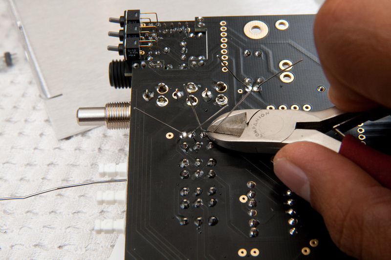
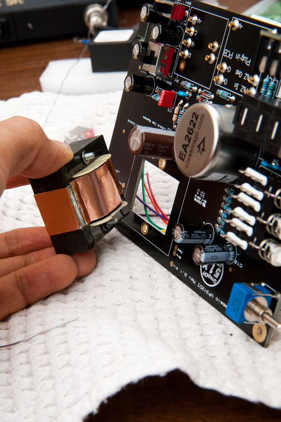
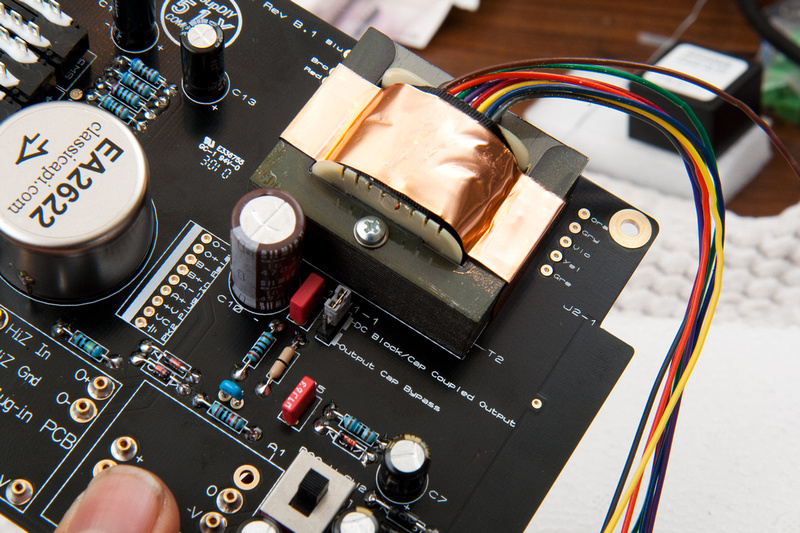
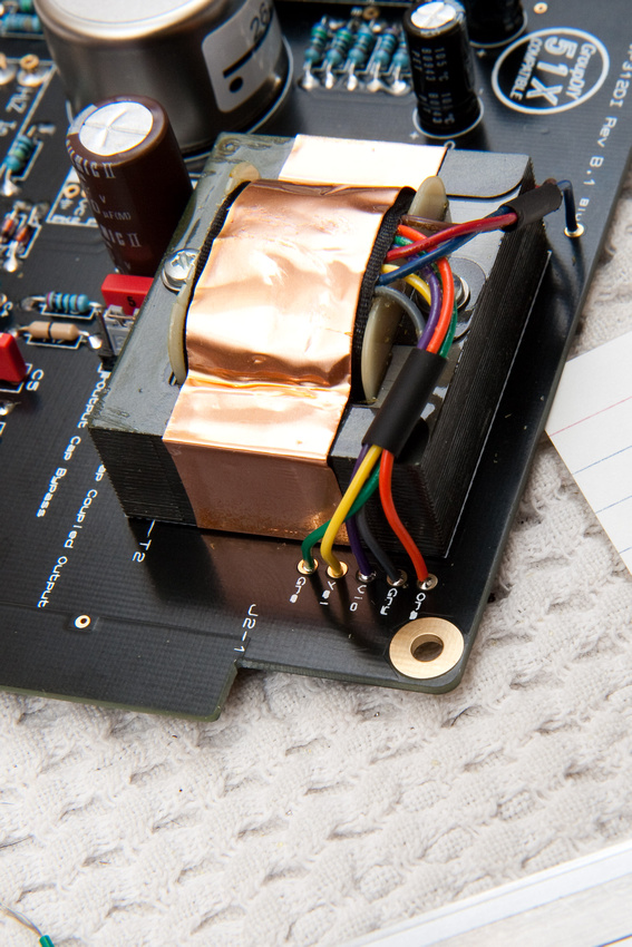
Then, you have to use your imagination a little bit and figure out where to cut the leads.

The 1st one of these is never going to be as pretty as subsequent builds, but since Jeff was kind enough to post actual cut lengths in the VP26 manual, I figure I'd go ahead and measure mine after I chopped them, stripped ~1/8" from the tips and tinned them with a little solder.
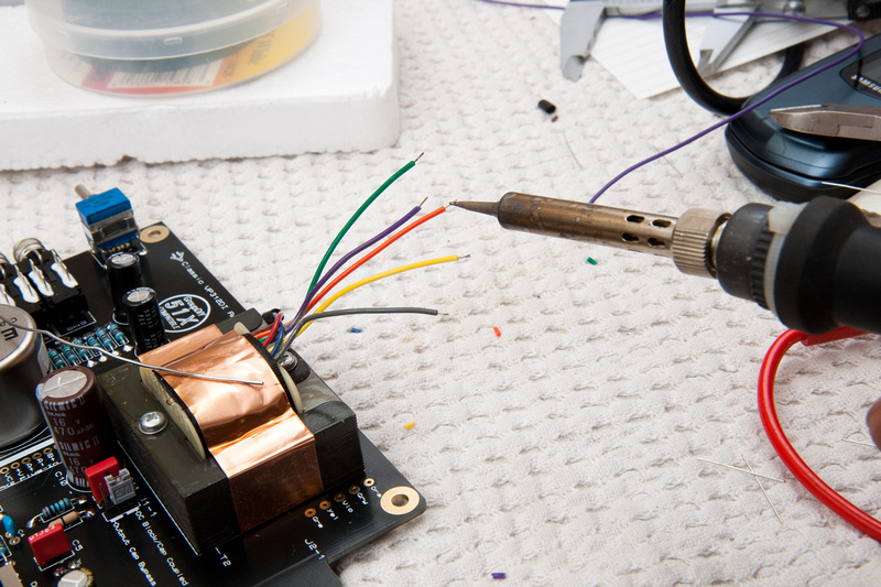
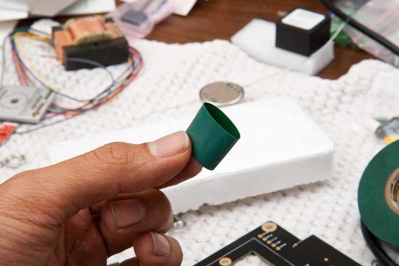
And, I used a couple pieces of shrink wrap to tidy things up a bit. . . completely optional IMO. It doesn't look stupendous, and it doesn't look horrible.
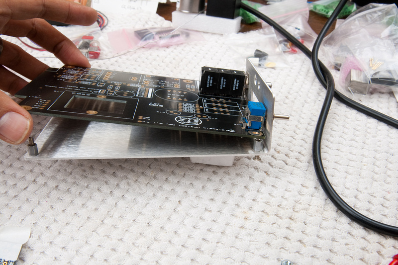
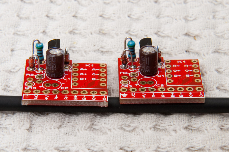
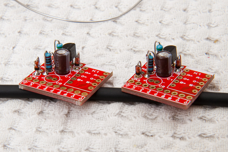
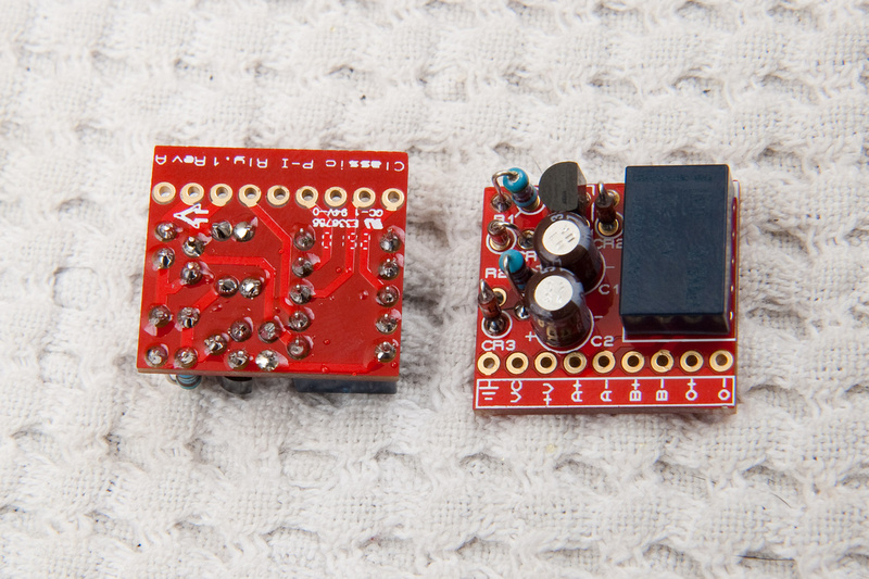
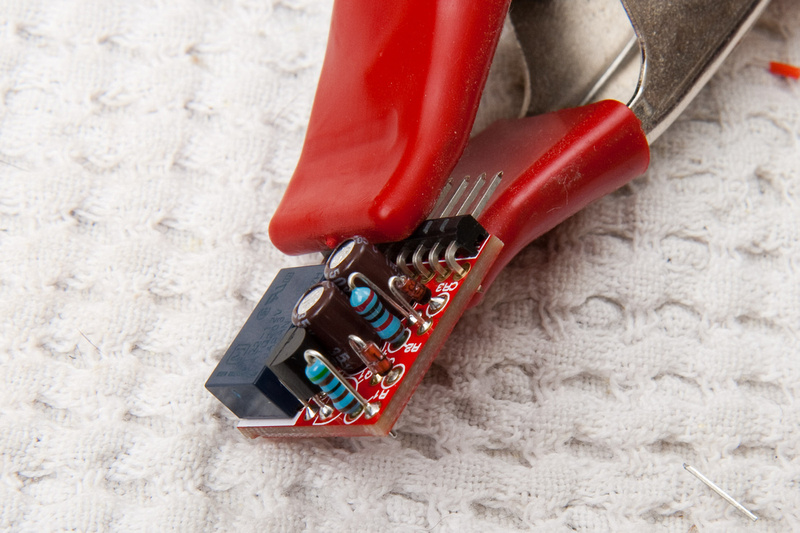
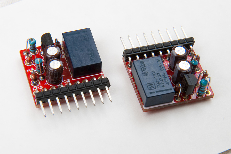
Next up, the 2 relay boards:
There is one diode here we haven't seen yet 1N749 4.3V which is CR1. It looks like this. . or, I hope it looks like this otherwise, I'm in big trouble.
labeled:
9C
4V3
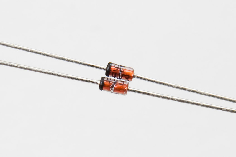
We've seen the other diode before 1N914 (CR2, CR3), but here it is again for kicks and giggles:
I decided to populate this board from top to bottom (similar to the GAR2520 kit)
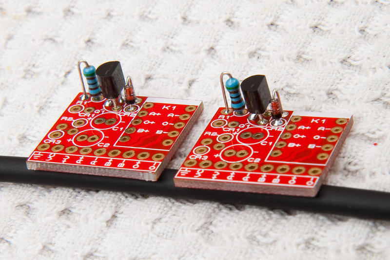
And, here's how I ended up holding the piece while soldering
Ok. . . I wasn't 100% sure about this, and I think those black box things are relays, but I aligned the white marking on top of the PCB with the marking on the black box thingies. If I'm wrong, I'm in for a world of hurt trying to get those guys out.
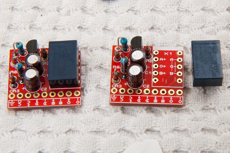
'Cause they're stuck on now pretty good.
next, find this piece in the appropriate baggie
I secured it to the relay board with a clamp.
I clamped all but 2 lugs and soldered the exposed lugs. . .
. . .then, I shifted the clamp to expose 2 lugs on the other side and soldered those. Then, I removed the clamp and soldered the remaining middle lugs.
Voila!
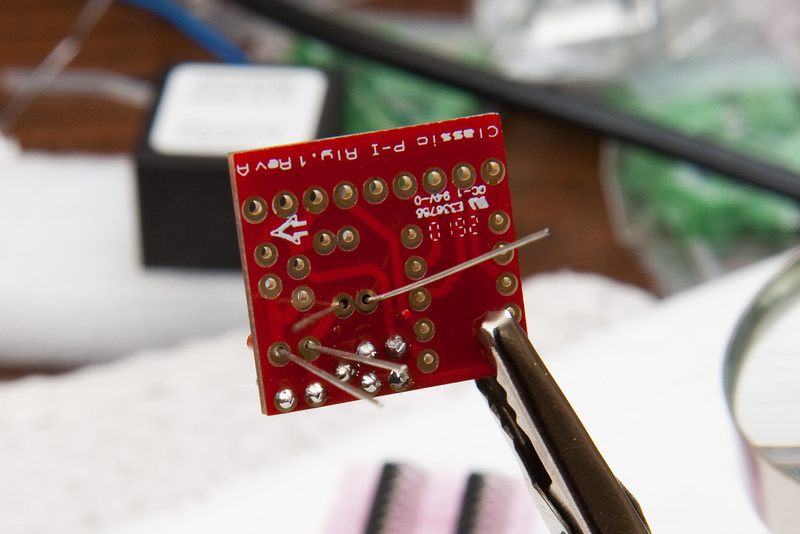
Pay attention to the markings that are now barely visible on the relay PCB's when installing. The DI relay board goes in here:
And the other one goes in here.
The relay boards are a bit tricky to install straight. Here's what I did. I put a small piece of loose packing foam under the relay board and then flip the PCB upside down.
The foam pushes up on the relay board, and I scootch things around until the relay board is more or less vertical and has solid contact on the PCB. Then, I solder from the back side.
Voila!
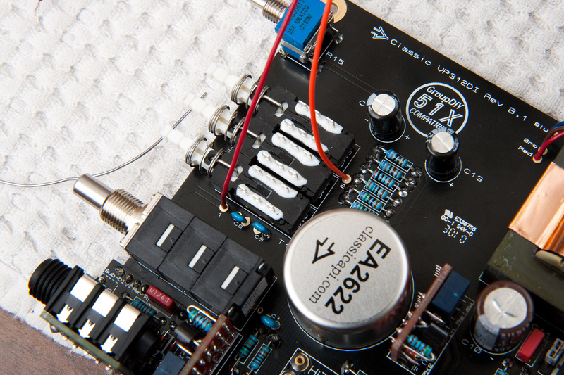
Next, I dug up the orange and red wires cut off from the output transformer and stripped/tinned one end:
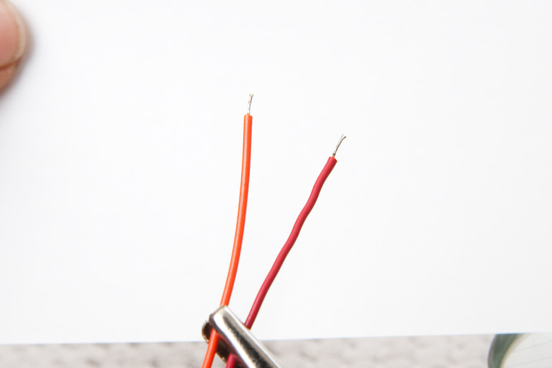
I then soldered them into the slots labeled "1" and "2" on the PCB.
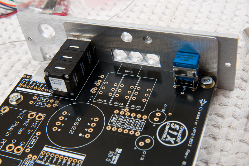
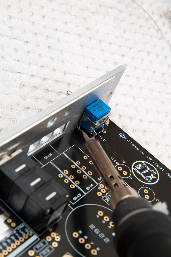
Next, I attache the PCB to the L-bracket and front face. Hopefully for the last time in a long while. The only difference this time is I use a lock washer between the nut and the PCB lug.
I then tighten down the front panel nuts to final torque. . .
then, I go dig the phantom power switch up from the appropriate baggie.
Install this with the lock washer between the switch body and the font panel so the switch has less tendency to rotate. (not pictured. . . oops)
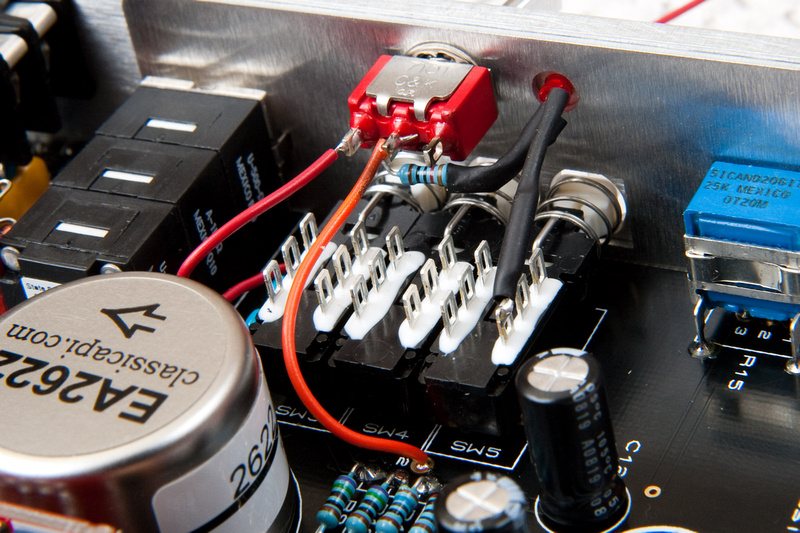
per Jeff's notes on the support thread, I bend the short end of the LED pins a little bit and put a piece of shrink wrap on it.
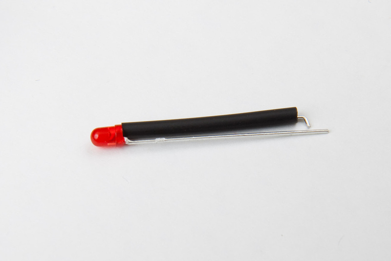
I then placed the LED and soldered the bent short end onto the last lead of SW5.
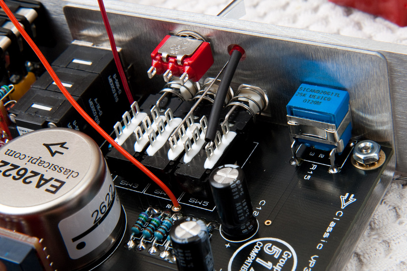
For the next part I deviate from the method outlined in Jeff's notes slightly. If figured for some non-existent reason that I wanted a more solid mechanical connection for the LED (in case of future dis-assembly when it's discovered i mucked something up).
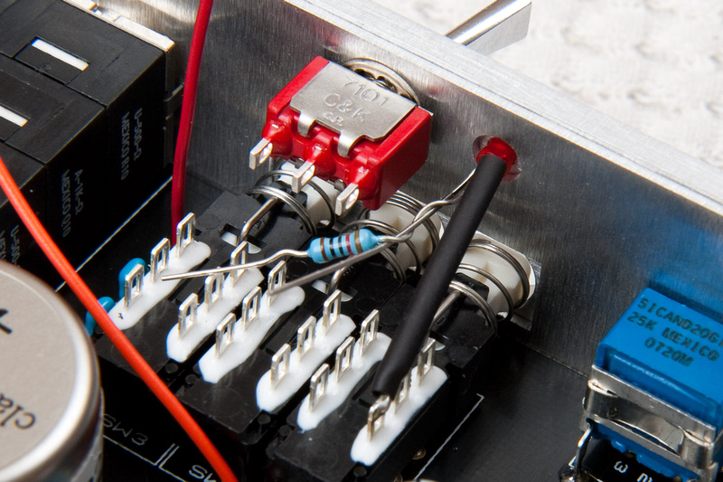
And Voila!
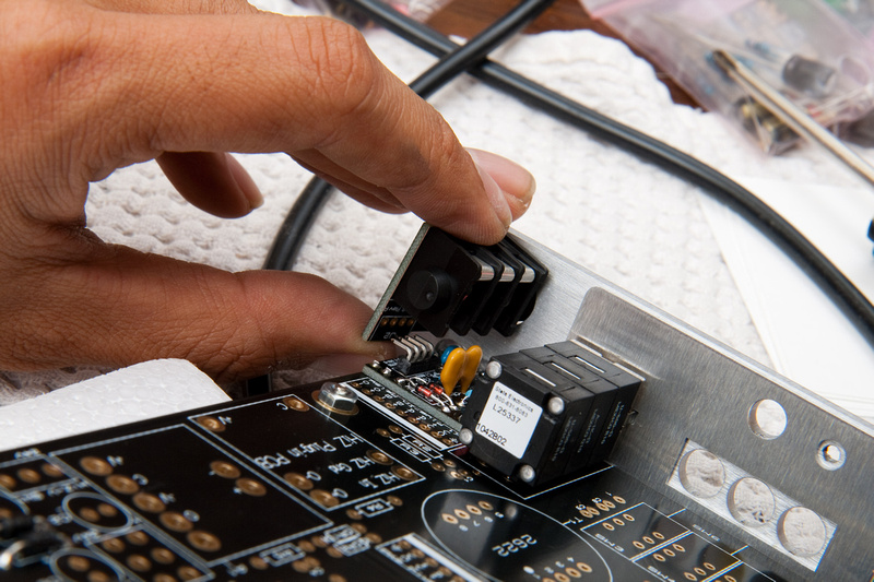
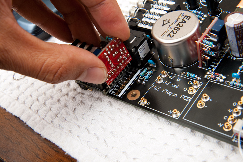
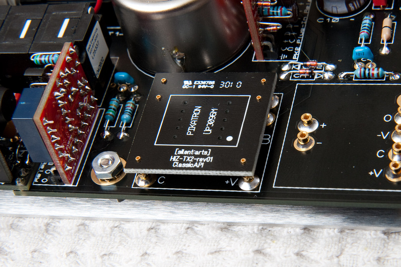
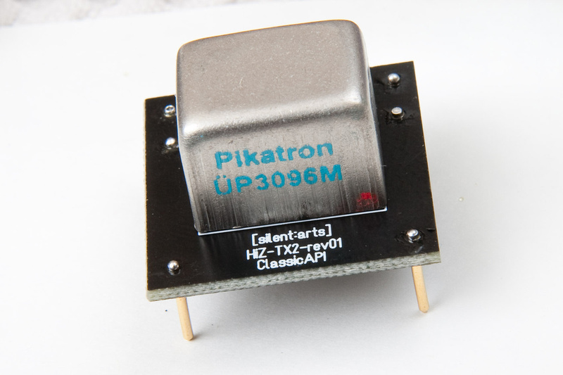
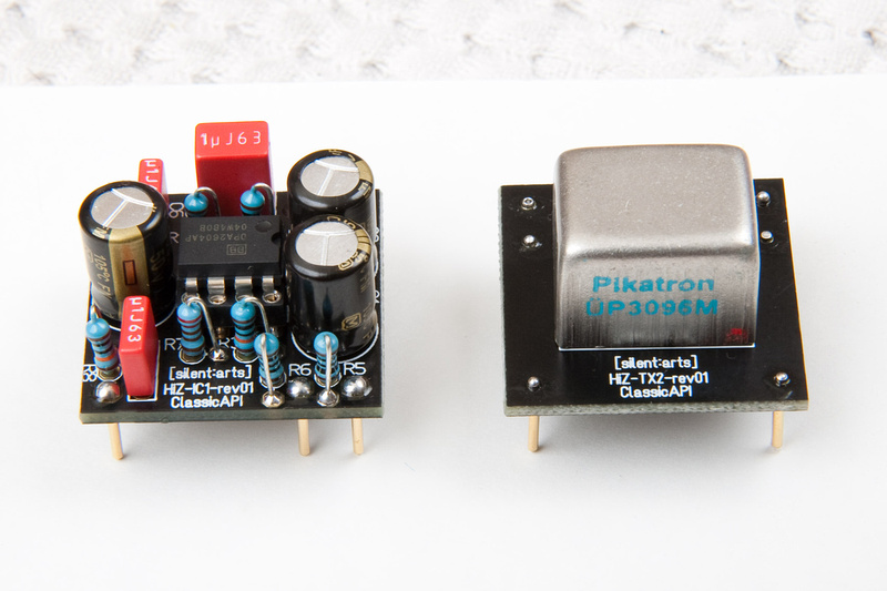
I was getting really tired at this point and wanted a "finished" preamp so I could pat myself on the back and feel good, so I looked at the baggies with the 3 preamp modules I had to try and find one with the least number of parts. . .
WINNER = Pikatron!
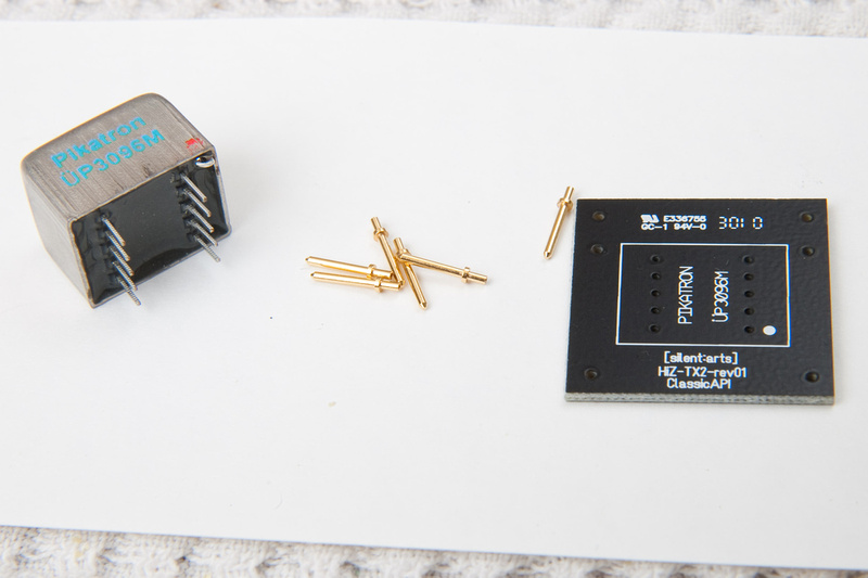
I shoved the pins into the appropriate slots on the PCB which was really difficult because the sockets are new. . . I ended up having to use small plug-in PCB to push down hard enough to seat the pins.
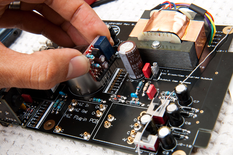
The pins were a pain to solder on because the Pikatron PCB is single sided. There are no lugs to solder to on the top side so initially, I relied on the solder that could creep down the pin to the back side of the PCB. When trying to extract the PCB from the socket (very difficult the first time), I ended up bending a good number of pins because one side released sooner than the other and very suddenly. . . but, this let me see how flexible and tough the little pins were. . . I ended up just soldering the pins "free" on the back side of the PCB so I could get a good mechanical solder joint on there and trust the pins are "close enough" to bend into the correct position when inserted. . . which worked out fine in the end.
Notice the rubbed off orange dot-ish marking on the pikatron transformer as well as the solder lug at pin 1. . . (or, I hope that's what I'm seeing). There is a corresponding dot on pin 1 of the PCB. Make sure these are aligned prior to soldering.
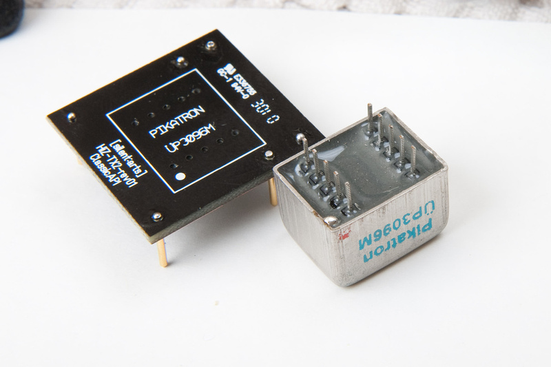
Pikatron complete. . . (notice slightly bent pins)
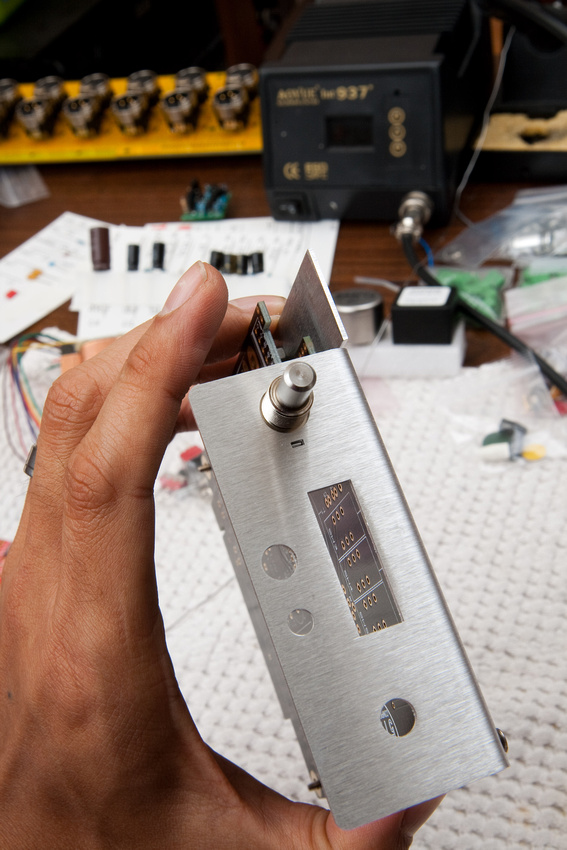
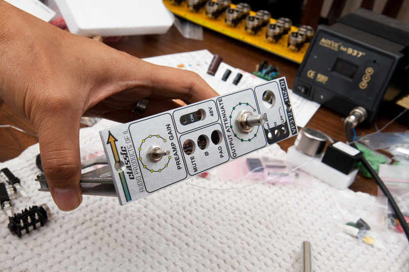
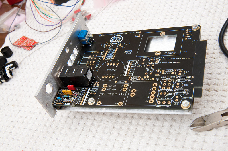
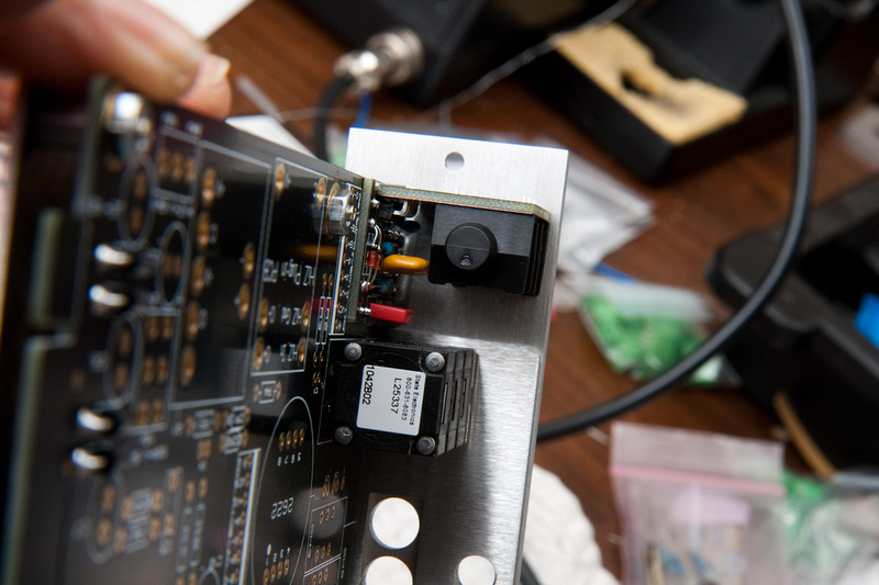
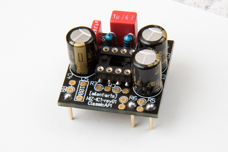
And, the preamp is now fully operational. . . well, in theory.
per the VP26 build manual, I used a dab of dish soap on the tips of the push switches prior to installing the white and black caps which helps those go on.
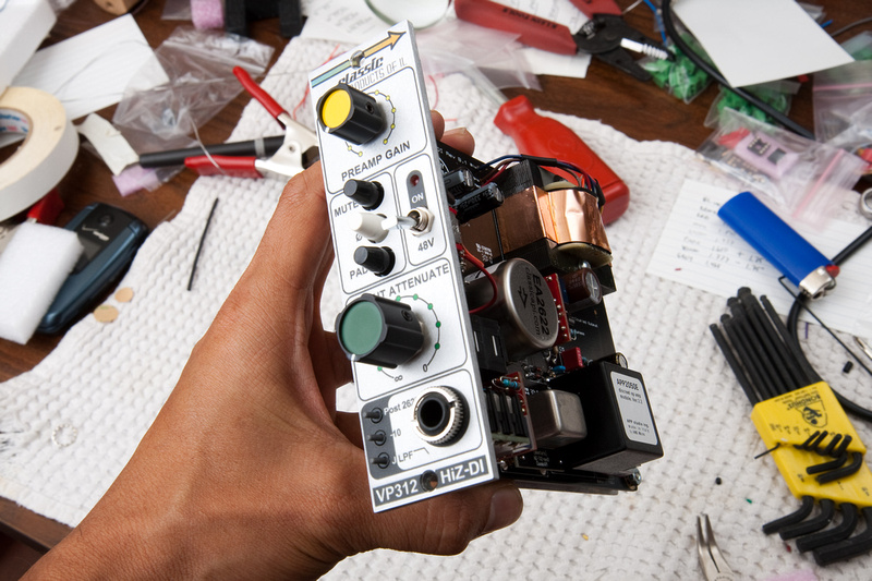
Humans win!
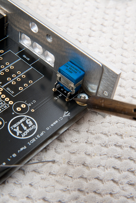
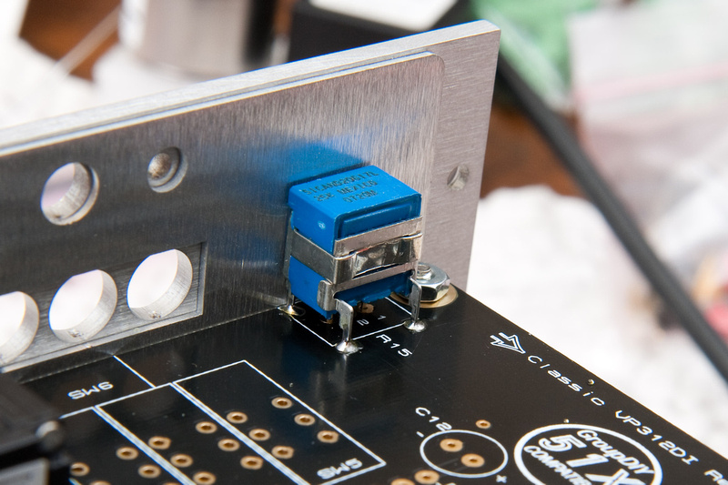
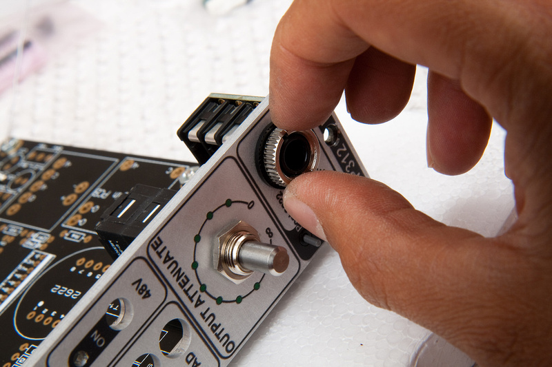
But then, I had a conversation with Jeff, and it seems I missed a cosmetic detail.
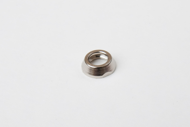
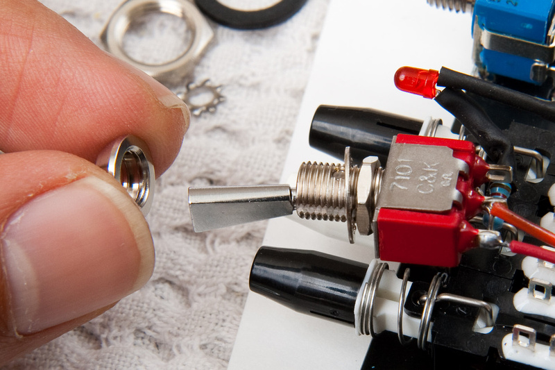
This is the nut that's supposed to be on the face of the 48V phantom power toggle switch. . . pretty. When I first took the toggle switch out, I couldn't get this nut to thread on, so I thought it must have been "extra parts". . . you know. . . like when you put your car back together.
Can't have my build not live up to expectations, so back in I go.
This is the proper setup. . . toggle switch --> nut --> lock washer --> L-bracket --> faceplate --> pretty nut.
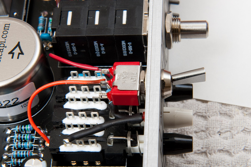
Much better. . .
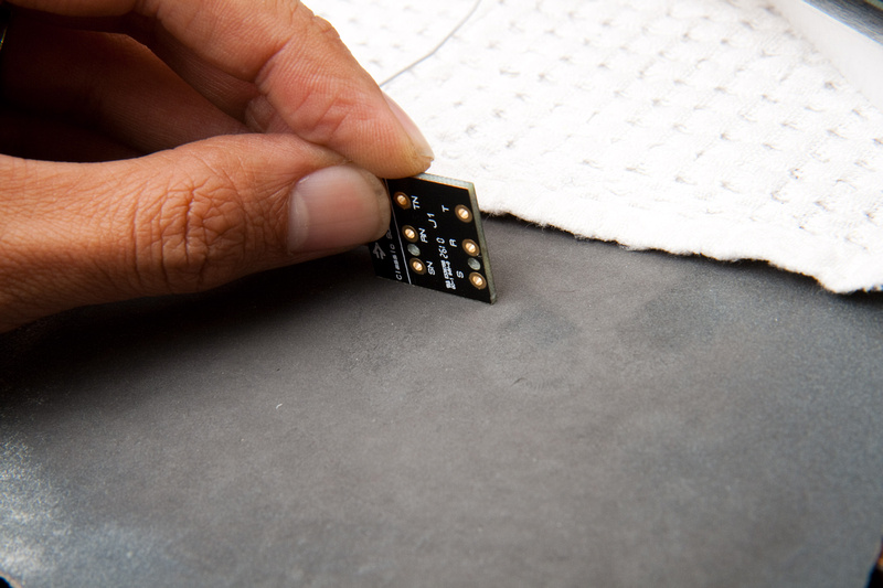
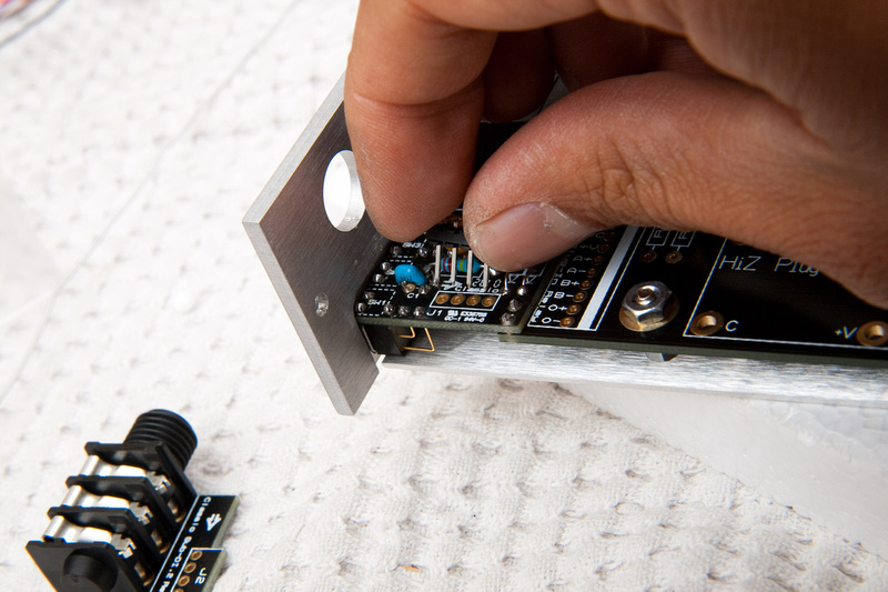
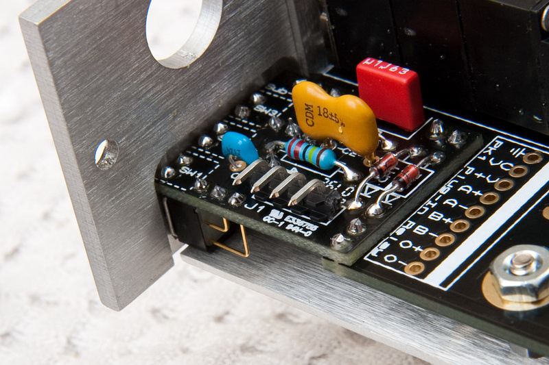
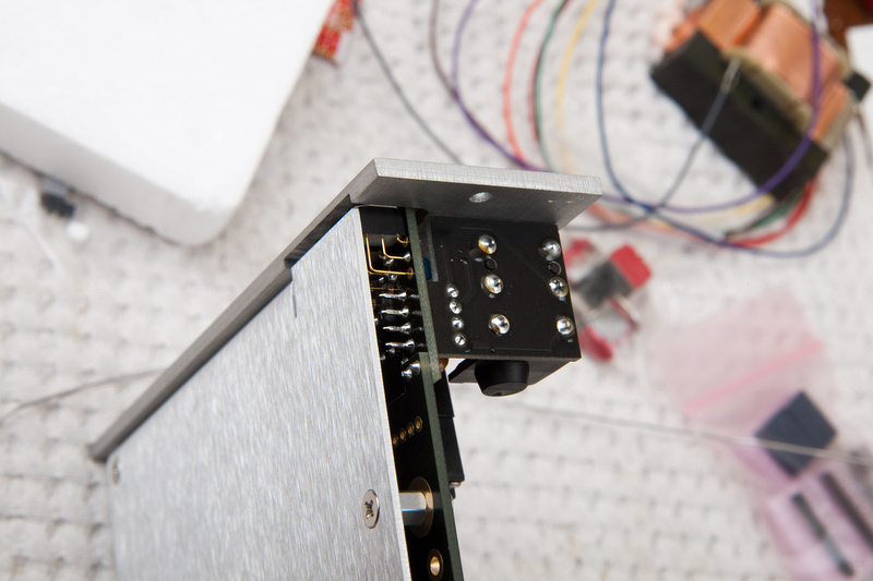
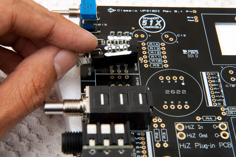
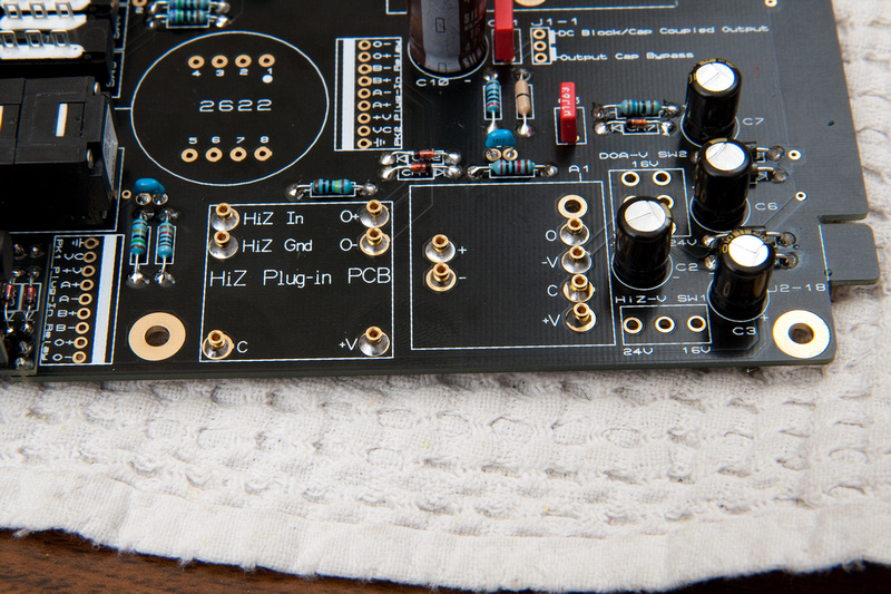
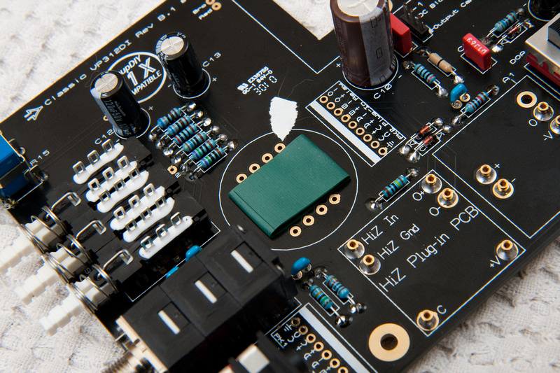
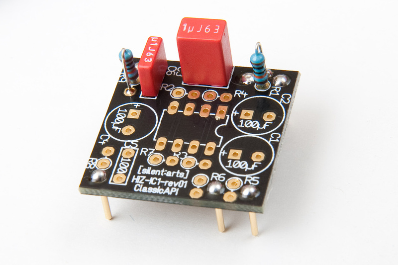
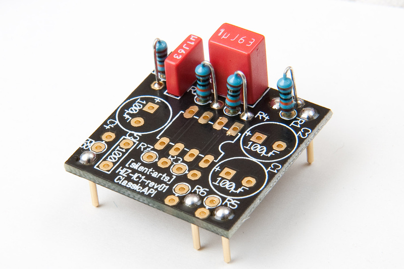
I decided to build the IC Direct Inject module next.
I started by putting the pins into the sockets. . .
Then, I placed the board on top of the pins and soldered.
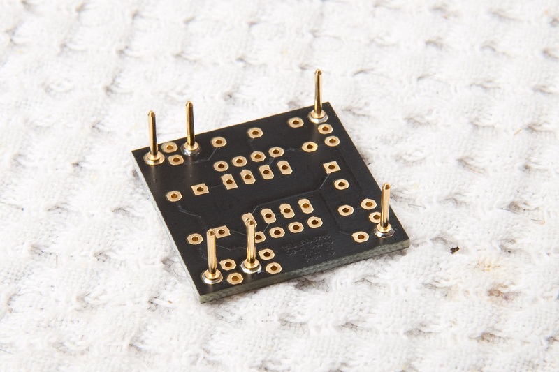
And. . .the sequence I stuffed the board in.
I rested the IC socket on something to hold it in place for soldering
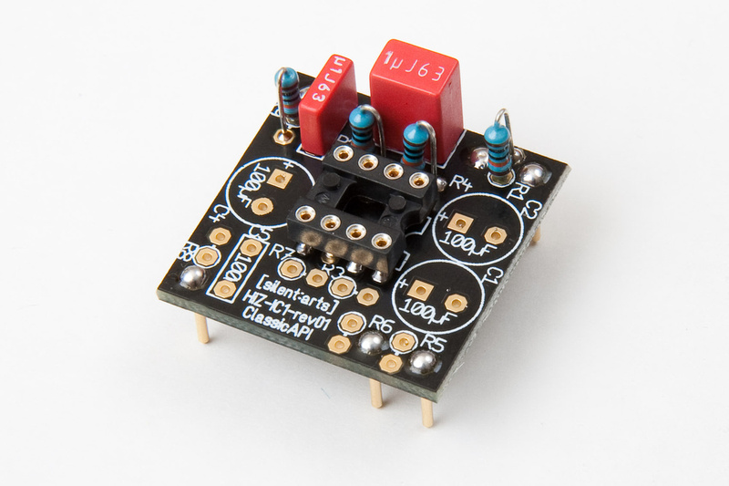
radial caps get soldered in. . .
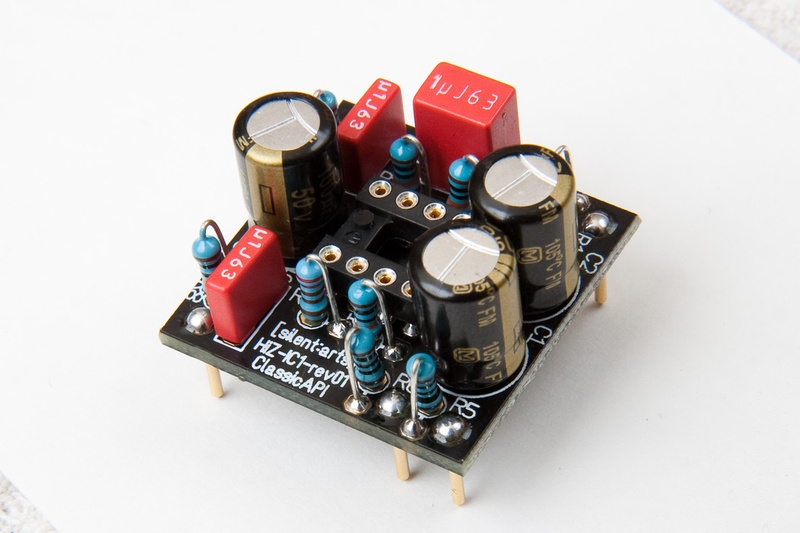
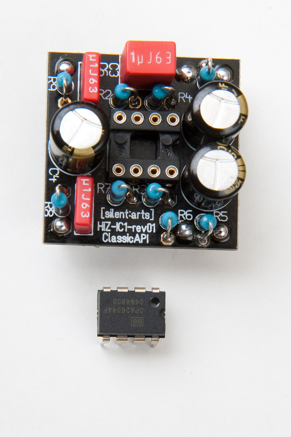
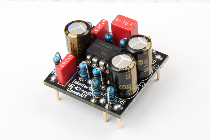

2 down, 1 to go.
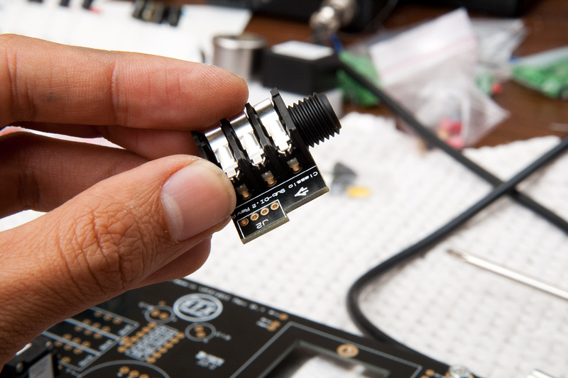
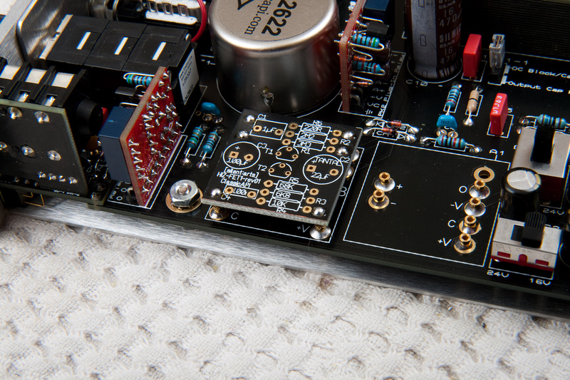
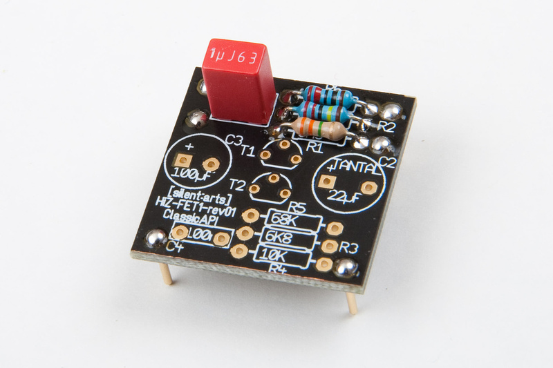
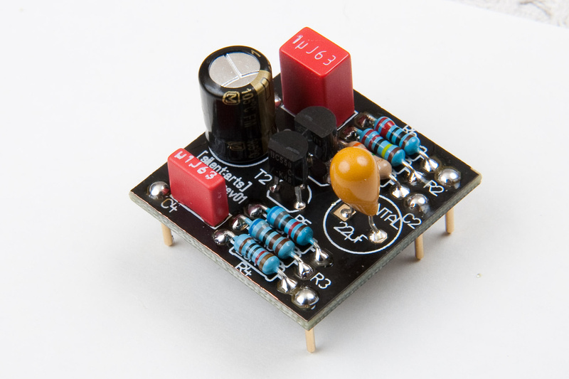
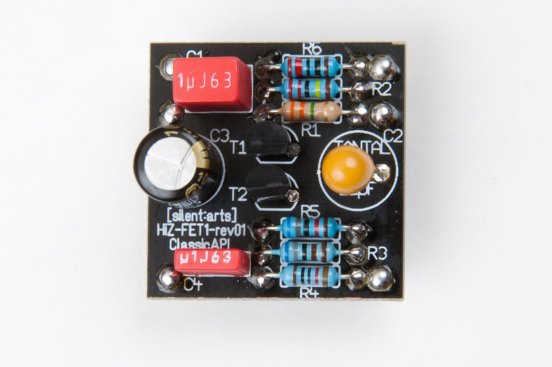
 The last HiZ Plug-in is the FET
one. Lucky for me, this one has no repeat parts so watch out. Every
component is different.
The last HiZ Plug-in is the FET
one. Lucky for me, this one has no repeat parts so watch out. Every
component is different.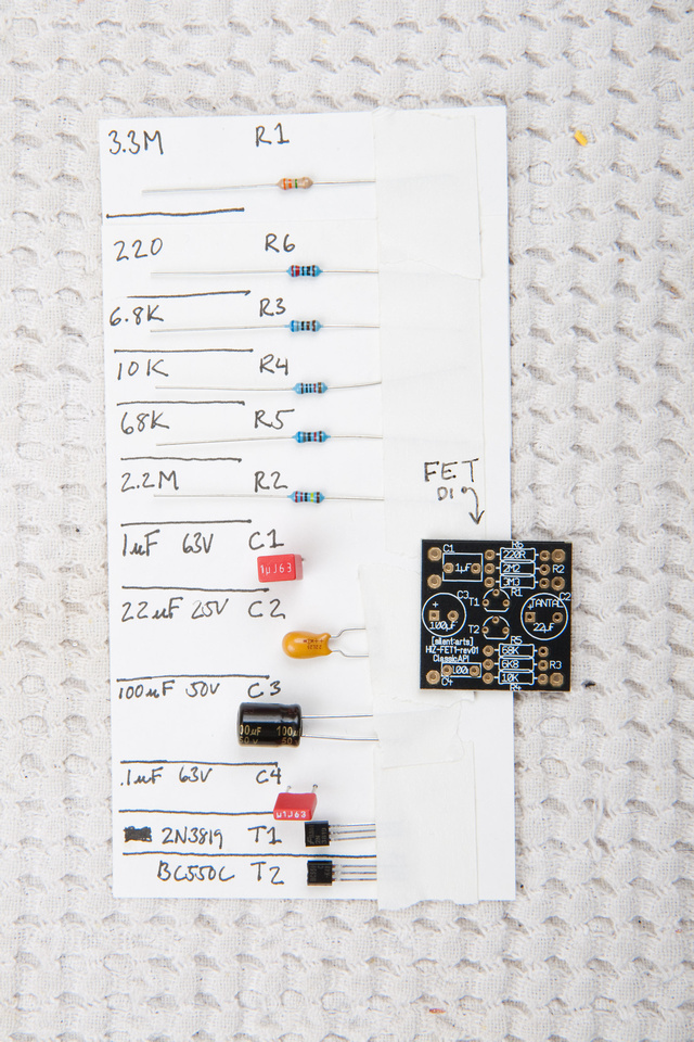
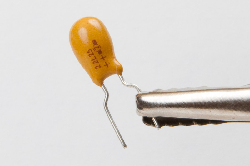
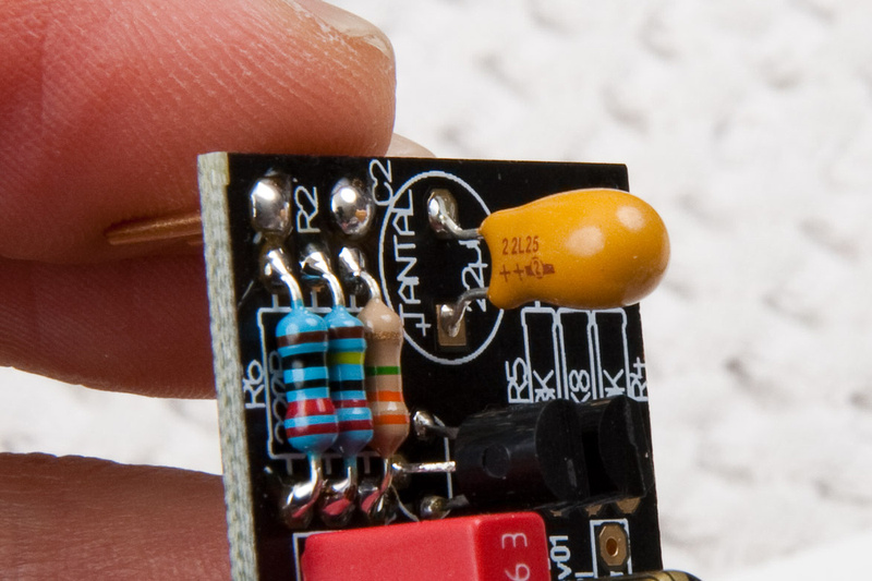
Watch out for this Tantalum cap (C2). It has to be installed with the correct polarity.
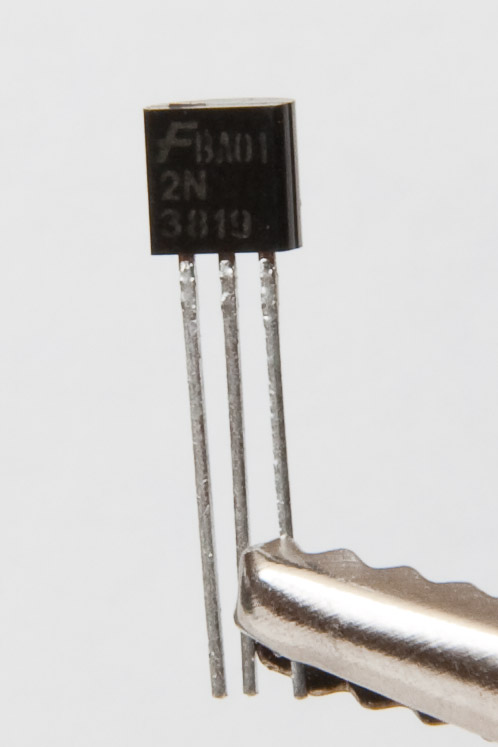
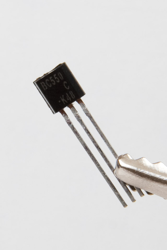
The 2 transistors are different (T1, T2) and the markings are hard to see.
I start again by inserting the pins into the sockets.
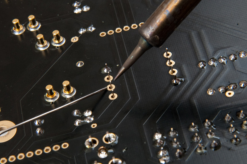
Then, I solder in the PCB with the pins aligned in the sockets making sure to heat the pin enough to flow some solder to the other side of the PCB for a better mechanical connection.
Then, I stuff the board.
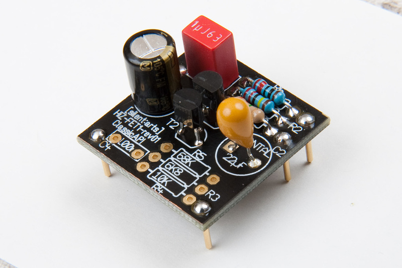
The tantalum capacitor has a marking for the + side. Make sure to line that up with the silk screened + mark on the PCB.
And, finished.
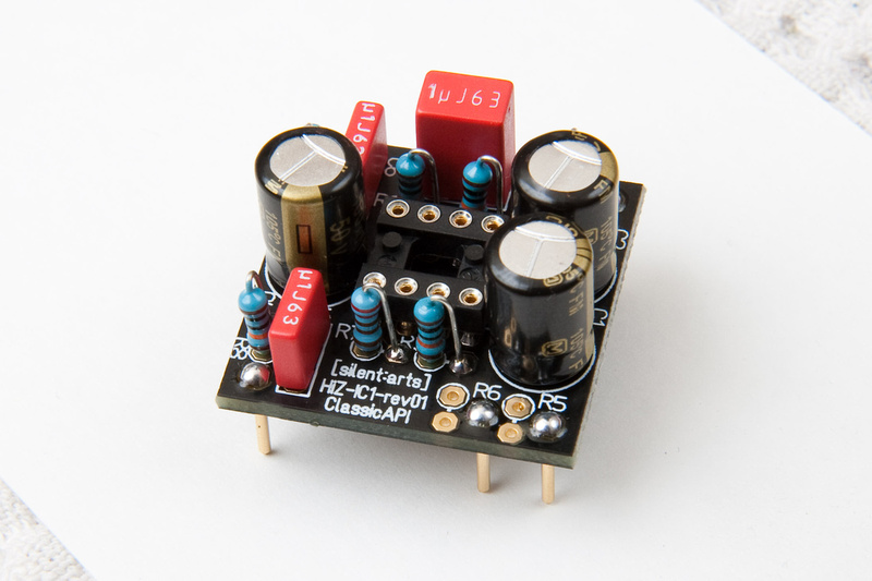
And then there were three
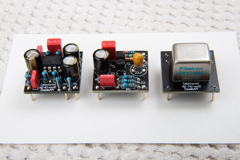
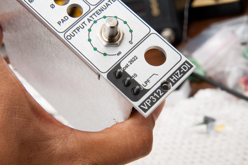
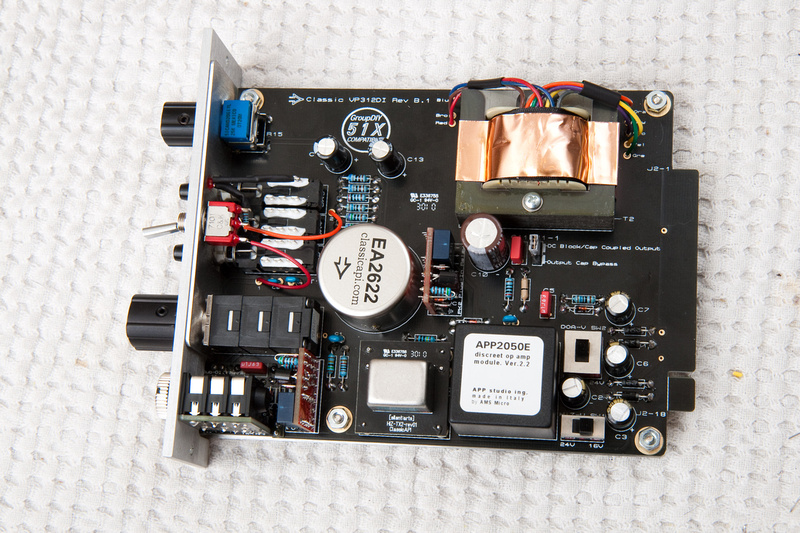
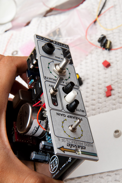
Project complete. This has to be one of the most customizable and configurable preamps in existence. I don't even have all of the modules. But, i do have a pair of gar1731's coming in so I'll be able to test those as well.
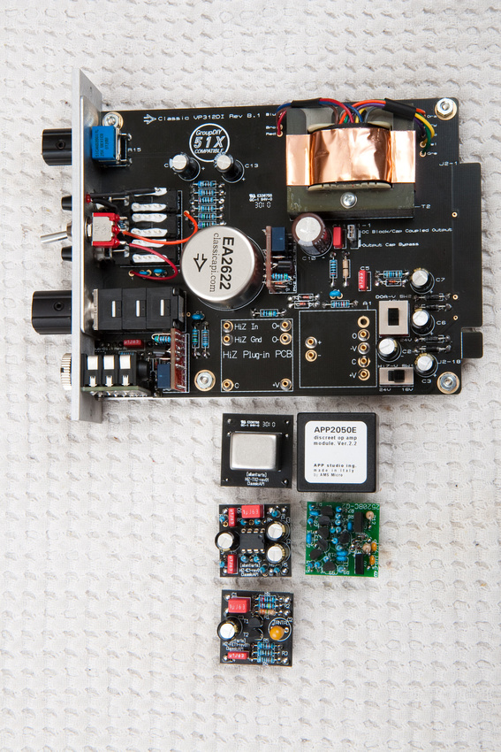
In the end, I liked the IC DI module the most. The FET unit is quite edgy to my ears, and in common applications like acoustic guitar pickups can get a little harsh. The Pikatron unit is pretty "down-the-middle", but seems to loose a little bit of detail and I like the gain of the IC DI module, so that is the one I have installed in this preamp permanently. At the end of the day, it was the GAR2520 that I liked in this preamp for most applications. The APP2050E does give a cleaner, more modern sound with GOBS or gain, but the VP312DI's serve most often in our studio connected to kick and snare, and for that specific application, the GAR2520 is fantastic.
No comments:
Post a Comment